

A Serial Data debugger is a tool used to test and debug other programs or target programs. This project is based on Atmega16A microcontroller (MCU), and is used to check the correct data received through universal synchronous/asynchronous receiver/transmitter (USART) interface on an LCD. It is a useful tool for debugging USART data for MCUs and related circuitry.
Generally, to check USART data of MCU, Rx and Tx pins are connected to COM port of the PC through voltage-level converters like MAX232. A program (for example, HyperTerminal) is then used to check correct data transmission on the computer terminal or screen. But, it is still difficult to check/identify non-printable characters on the computer screen. These days, a COM port is not available on PCs and laptops, and more hardware setup is needed for USB to COM port conversion.

This simple and handy serial data debugger can solve the problem. In this project, instead of COM port two similar circuits are wired to transfer the serial data for testing.
Circuit and working
The circuit diagram of the serial data debugger is shown in Fig. 1. It is built around ATmega16A MCU (IC1), 16×4 LCD (LCD1) and a few other components.

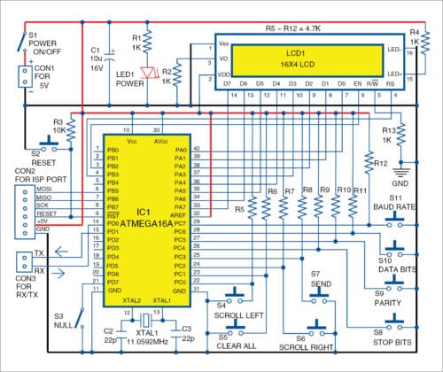
ATmega16A employs a 11.0592MHz crystal to have accurate baud rate. LCD1 is used as output/console.
USART frame size/format can be varied as per requirement by pressing such buttons as baud rate (S11), data bits (S10), parity (S9) and stop bits (S8). This frame detail will be displayed on the fourth line of LCD1. Use null switch S3 to enable or disable null values to be added to the buffer while receiving the data stream.
Two circuits (say, MCU1 and MCU2) of Fig. 1 are wired on a separate PCB. Their Tx and Rx pins are connected to each other. Serial data is sent by MCU2 through its Tx pin and received by Rx pin of MCU1. Serial data is written to a buffer in MCU1 for debugging received data. Maximum buffer size is 255 characters.
Each buffer position and its byte data occupy two columns of LCD1. So, LCD1 can display eight-character data of received buffer at a time.
First row of LCD1 displays position of the buffer in hexadecimal format, second row displays actual character, third row displays data in hexadecimal format and fourth row displays frame size of data being received.
To scroll through data, use scroll left (S4) and scroll right (S6) buttons. Data in the buffer can be studied comfortably. By pressing clear all (S5) button, all data in the buffer and screen will get cleared, and new data will be received and displayed on LCD1. The number of characters received is displayed on the right-bottom of LCD1.
To send a data stream, press send (S7) button. String/data stored in send_data (in the code) will be transmitted through Tx pin of the MCU.
Setup and self-test
After successfully assembling the circuit on the breadboard or PCB, write SerialDataDebugger.hex file to ATmega16A (IC1) and set fuse bits for crystal option (ckopt=1, sut0=0,sut1=1,cksel0=1,cksel1=0,cksel2=0,cksel3=0) through ISP port using AVR programmer. (Refer Atmel data sheet for full details.) Note that a fresh MCU has a default value of fuse bytes, which is equal to 0X99E1 in hexadecimal.
For testing the programmed MCUs, connect Rx and Tx pins of IC1 (MCU1) to Tx and Rx pins of MCU2, respectively. Power on both units, and press send (S7) button on MCU2. Data/string stored in send data buffer should appear on LCD1 of MCU1. Disconnect Rx and Tx pins, and the serial data debugger will be ready to use.
For power supply, use a 5V power bank of 2000mAH or higher capacity, which is rechargeable and makes the complete circuit handy.

Construction
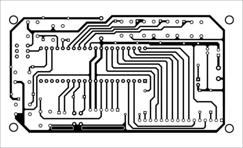
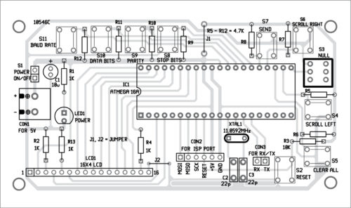
A PCB layout of the serial data debugger is shown in Fig. 2 and its components layout in Fig. 3. Assemble the circuit on the designed PCB and connect 5V DC across CON1. CON2 is used for programming Atmega16A using any ISP programmer. CON3 is used to connect transmitter (Tx) and receiver (Rx) pins from another MCU.
After assembling and testing the circuit, enclose it in a suitable cabinet. Fix the switches, LCD1 and LED1 in front of cabinet. Keep 5V, 2000mAh power bank inside the cabinet.
PCB and Component Layout PDFs: click here
For downloading source code: click here
Note
Rx of IC1 should be connected to Tx of another MCU and vice-versa.
Fayaz Hassan is manager at Visakhapatnam Steel Plant, Andhra Pradesh. His interests include MCU projects, mechatronics and robotics