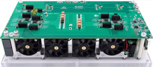
The SiC-based isolated DC-DC converter design with 30 kW output is optimised for EV chargers and high-power applications. Learn more!

A SiC-based polymorphic DC-DC converter is a power conversion system used in high-power applications where efficiency, compactness, and reliability are important. These converters use SiC semiconductors to handle higher voltage levels, operate at higher frequencies, and reduce power losses compared to traditional silicon-based systems.
The polymorphic design allows for flexible voltage conversion in various settings, such as electric vehicles, renewable energy systems, and industrial automation.
The evaluation board from Microchip is designed to demonstrate the performance of a SiC-based isolated DC-DC converter, showcasing the capabilities of SiC MOSFETs and diodes.
The isolated DC-DC converter design is tailored for Hybrid Electric Vehicle (HEV) and Electric Vehicle (EV) chargers, along with high-power switch-mode power supply applications. By incorporating 1200V SiC MOSFETs and SiC Schottky Barrier Diodes (SBDs), the reference design achieves a 98.5% efficiency and a power density of 7.2 kW/L at 30 kW output power. Using this reference design, design engineers can evaluate the performance of SiC MOSFETs and diodes in high-power DC-DC conversion systems, gaining insights into their efficiency, voltage handling, and switching capabilities.
High-voltage direct current (HVDC) applications, such as external fast DC chargers, industrial power systems, data centre and telecommunications power, and battery backup systems, benefit from the converter’s ability to efficiently and reliably transmit power over long distances in high-demand environments.
The design is optimised explicitly for 30 kW applications, using an isolation asymmetrical dual full-bridge topology. This PSFB DC-DC converter topology is well-suited for 400V EV systems and high-voltage power sources.
The SiC-based DC-DC converter, with its isolated power configuration, also features a PCB layout designed for safety, current and mechanical stress, and noise immunity.
On the primary side of the converter, two constant-frequency full-bridge sections are implemented, referred to as the leading and lagging H-bridges. Depending on the input and output operating conditions, each H-bridge can function as a full-bridge or half-bridge.
The additional H-bridge configuration enables the converter to operate as a full-bridge with a phase shift between the leading and lagging H-bridges or as two half-bridge controllers with a phase shift between them.
Additionally, the design allows phase shifting within a single H-bridge configuration. This topology supports a wide 4:1 output voltage range and maintains Zero Voltage Switching (ZVS) throughout all operating conditions, ensuring high efficiency.
The converter can be controlled similarly to a buck converter using a carrier-based modulation method. The system senses output voltage and current, which are input into a Proportional Integral (PI) controller to regulate the output power.
The converter supports two operational modes: Constant Voltage and Constant Current, both of which can be easily configured using the control software, providing flexibility for various applications.
Microchip has tested this reference design. With the included bill of materials (BOM), schematics, assembly drawings, and PCB layouts, engineers can quickly prototype and test their designs, accelerating the development process for high-efficiency power conversion applications. The company’s website has additional data about the reference design. To read more about this reference design, click here.


