 This project helps you build a 8-Bit computer while also providing an insight into the working of an MPU & its construction mechanism.
Computers take an input, process it as per a set of instructions and provide the output. These are general-purpose devices that can be programmed to carry out a set of arithmetic or logical operations automatically.
Intel 8008 was the first 8-bit microprocessor for the microcomputer system. The architecture of a microprocessor seems complex, but a computer can be entirely built with TTL logic chips without using any microprocessor/controller. This project helps you build your own computer while also providing an insight into the working of a general-purpose microprocessor as well as its construction mechanism.
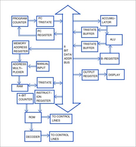
Architecture
This 8-bit digital TTL computer is designed as per the architecture shown in Fig. 1. The entire processor circuit is powered from an SMPS as it consumes a lot of power. Voltage supply is 5V.
The architecture has a common 8-bit bidirectional data/address bus. The arithmetic logic unit (ALU) consists of adder/subtractor circuit along with AND, OR, NOT and XOR gates to perform logical and arithmetical operations. The values for operation are stored in A-register (Accumulator) and B-register. The number of states and sequence of states for all the instructions are stored in the ROM. Two ROMs are used to control the sequence of operation for various modules in the system. ROMs provide 16 control lines for operation.
The output and enabling of different modules are controlled by EN pins of ICs or tristate buffers. For example, the ALU output is controlled by using tristate buffer at the end of each logic output. The ALU output selection based on the instruction is done by a decoder connected to ROM2 as shown in the circuit diagram Fig. 2.
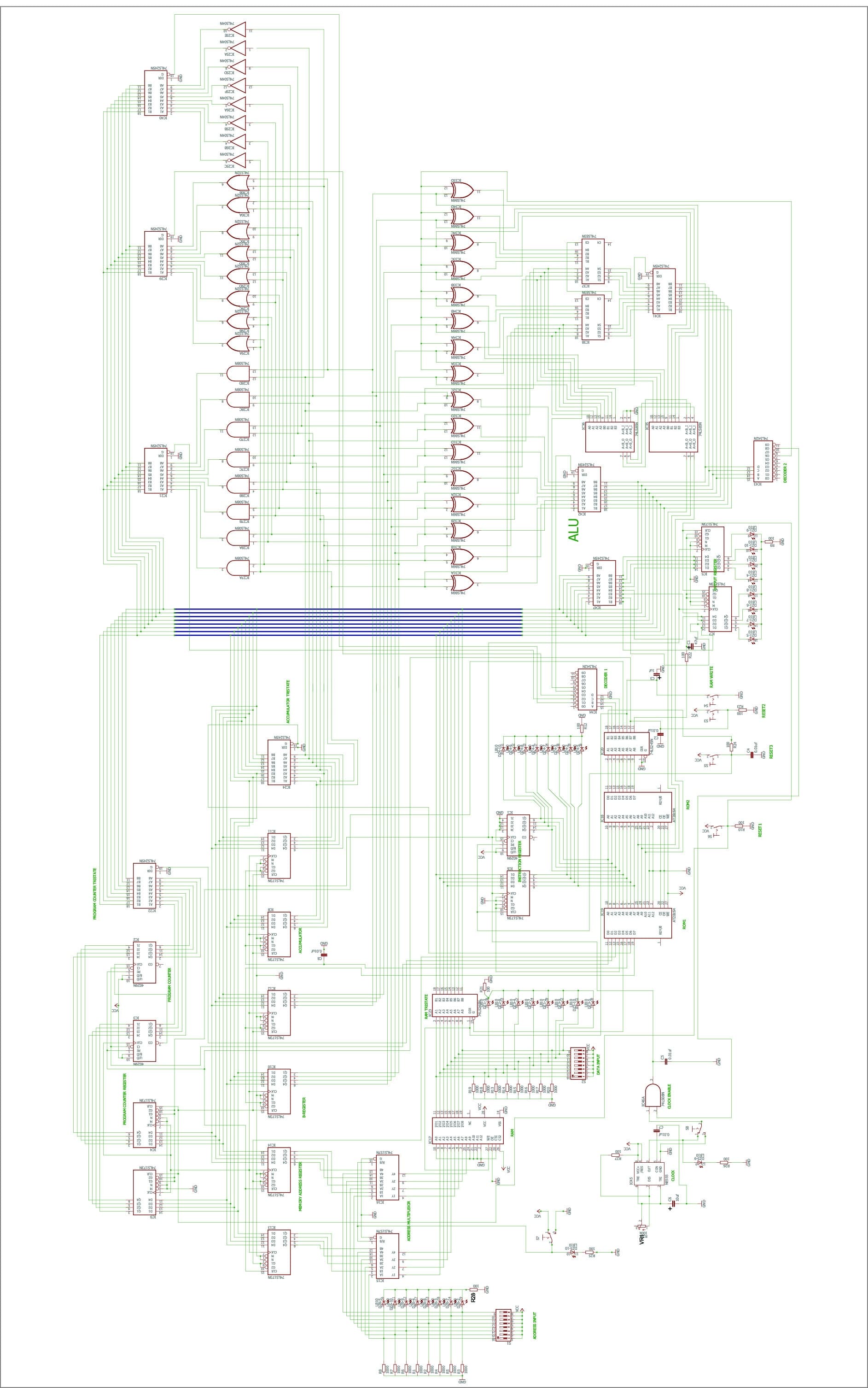
Download circuit
Typically, the sequence of operation is as follows:
1. The program counter (PC) is incremented
2. The PC value is loaded in the memory address register
3. The instruction is stored in the instruction register of the RAM at the address specified by the memory address register
4. The PC is incremented
5. The memory address register is updated with a new PC value
6. The LDI instruction loads the data in the accumulator specified by the memory address of the RAM
7. The instruction register is cleared for next instruction loading
The author’s prototype with five LED bar displays is shown in Fig. 3. LED bar displays show the status of output, data, address, instruction set and state. This helps in tracking how each instruction is being executed.
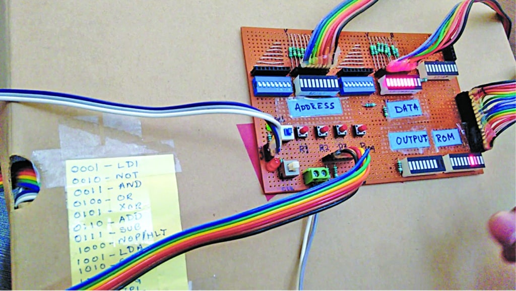
Circuit and working
As can be seen from Fig. 2, inputs to the accumulator, B-register, output register, PC register and memory address register are fed through the 8-bit parallel address/data bus. The input to the ALU is provided by the accumulator and B-register.
The ALU outputs to the bus via tristate buffers. The accumulator also outputs to the bus via tristate buffer 74LS245N. The tristate buffers are controlled by enable (G) pin.
The PC register output is fed to the program counter, providing the value to be loaded in the counter. The PC outputs to the bus via a tristate buffer. The memory address register outputs to the multiplexer.
The multiplexer output is fed to address pins of the RAM (CY6264). Input/output pins of the RAM are connected to the bus via the tristate buffer (IC23). The DIR and G pins of the tristate buffer are controlled based on the instruction and data flow. The 4-bit LSB of the bus is fed to the instruction register (74LS173N).
The inputs to the counter (CD4029N) are grounded. The outputs of the instruction register and the counter are connected to the address pins of ROMs (AT28C64). The ROM outputs are connected to enable pins of various ICs to control the data flow based on the state and instruction.
The functions of different modules in the architecture are as follows:
Program counter.
The program counter provides the computer with the current address of the instruction to be executed.
Memory address register.
The memory address register (MAR) stores the current address for the byte to be read or written from the memory.
Multiplexer.
The multiplexer allows selection of address either from the MAR (in run mode) or the manual input (programming mode).
Instruction register.
The instruction register of a computer stores the current instruction that is being executed.
During the computer’s operation, the value stored in instruction register is the instruction opcode. It forms the four bits of middle-value address (A4-A7) for ROMs. The counter for the next state provides the four bits of LSB (A0-A3) for ROMs. The 3-bit output from the comparator (74LS85N) forms the MSB (A8-A10). Thus, the address (A0-A10) is fed to the two ROMs to generate the control logic for different modules.
Output register.
It stores the value of the accumulator and displays the result.
Clock. The clock pulse is generated by an NE555 timer chip configured in astable mode.
ROM control
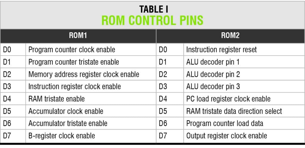
The two ROMs along with a 3-to-8 line decoder (74LS42N) provide a total of 18 control lines that control, enable or reset different parts of the computer. These control the clock enable pins of chips, thus controlling the data/instruction flow between various parts of the computer. The decoder output controls the tristates of the ALU controlling the data flow of the ALU result into the bus.
The ROM address is fed by the instruction register and counter. The data against the address for each state in the ROM is provided through the control lines or input/output pins. The functions of ROM control (I/O) pins, as per the schematic in Fig. 2, are listed in Table I.
Programming
Programming this computer is simple. There are two on/off switches (S8 for clock on/off and S7 for program/run mode selection), four pushbutton switches (S3 through S6) and two 8-bit DIP switches (one for address and the other for data). S3, S5 and S6 are reset switches, while S4 is RAM-write switch.
Toggle switch S7 to ‘program’ mode. The LED connected to it should turn off. Switch the clock to ‘off’ mode. Switch 8-bit address to the first address (0b00000001) and set the data DIP switch to the instruction/data to be written on the address. Press RAM-write switch S4 to load data onto the address. Similarly, repeat the process for successive code lines.
After entering all the codes/inputs, toggle program/run switch S7 to ‘run’ mode. Reset switches S3, S5 and S6 to clear all the LEDs. Press switch S8 on the clock to start computation. The maximum number of code lines that can be written for this project is 255.
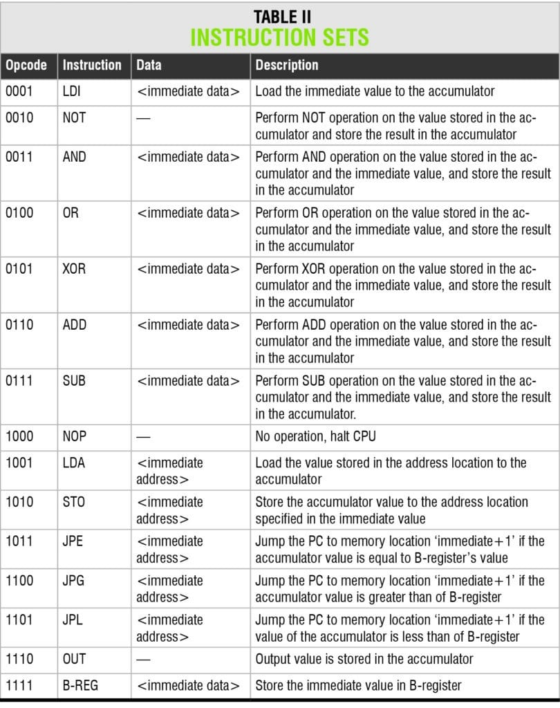
Various instruction sets are listed in Table II.
Example.
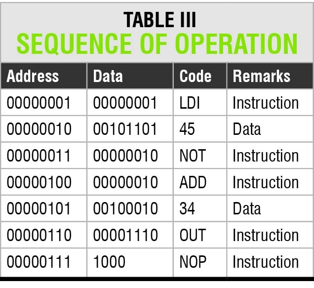
The following code loads 45 in the accumulator, performs NOT operation on it, ADDs 34 to the result, displays the output and halts:
LDI 45
NOT
ADD 34
OUT
NOP
The sequence of operation is as follows:
1. Stop the clock mode
2. Clear all resets (press reset 1->2->3->1 or press S6->S3->S5->S6)
3. Switch S7 to ‘program’ mode
4. Set address to 00000001 using DIP switch
5. Set data DIP switch to value 00000001
6. Press RAM-write button S4
7. Set address DIP switch to next address 00000010
8. Set data DIP switch to value 00101101(binary for 45)
9. Press RAM-write switch S4
10. Repeat it until the NOP (00001000) is set in the RAM
11. Switch S7 to ‘run’ mode
12. Start the clock using switch S8
The sequence of operation is shown in Table III.
LDI instruction flow diagram (not shown here) is included in source folder.
ROM code
The address from the instruction register, counter and comparator is fed to the two ROMs.
The ROM code is provided in a separate file in the source folder.
Burn the exact code into ROM1 and ROM2. For details on burning the ROM code, refer the datasheet of AT28C64. All the ROM address fields must be filled with the following values to ensure there is no garbage value for any random ROM address:
ROM2 ROM1
0b11111111 0b10110001
Challenges faced during project design and development
1. Designing the CPU architecture required logic implementation for modules and blocks
2. Programming the ROM for control logics during state change of a particular instruction
3. Fan In and Fan Out issues while driving logic signals in multiple chips
4. Noise and signal inductance issues in the circuit
5. Determining the minimum states required for each instruction and modifying the architecture accordingly
6. Determining the sequence of operation for clearing different modules
7. Issues of common address/data bus architecture
8. Prototyping complex logic on the PCB/breadboard
Advantages of the project
1. Helps gain an understanding of the working of a microprocessor (all modules and instruction flow between modules)
2. Useful substitute for microprocessor trainer boards
3. Programming (feeding instructions and data) is easier
4. Clock speed can be adjusted to monitor instruction/data flow in the computer
5. Multiple displays provide the CPU information
6. In case of malfunction, IC replacement is cheaper and easier
7. A perfect kit for hobbyists and computer enthusiasts interested in retro programming/computing
Disadvantages
1. Instruction set limited to only 16
2. Displays are LED bar type, not 7-segment/readable
3. Input is through DIP switches, which is not very user-friendly
4. Program needs to be written every time the CPU goes off
5. Maximum result is 255 (8-bit only)
Download source folder


Nice job. I also interested in building my own computer, even it can be a 4-bit or 8-bit, but I want to build it from zero like you did. It’s a good idea to use arithmetic ttl chips. But have you ever thought to use 74LS181 ALU chip? Why did you choose the messy arithmetic chips instead of an ALU chip? Thanks