


 This circuit protects the power plug of a switched-mode power supply (SMPS) against sparks that may damage its contact terminals. It normally happens when the device (laptop charger, mobile charger, etc) is plugged to a multi-socket board whose power is already turned on. Under this condition, while plugging in the SMPS, the capacitor (which is present in the initial stage of the power input circuitry) inside it conducts heavily for a short time, virtually short-circuiting power terminals L and N.
The time of short circuit depends upon the time constant of the circuit formed by the input capacitor and resistor. It can cause a heavy spark between the plug terminal and the socket causing damage to both.
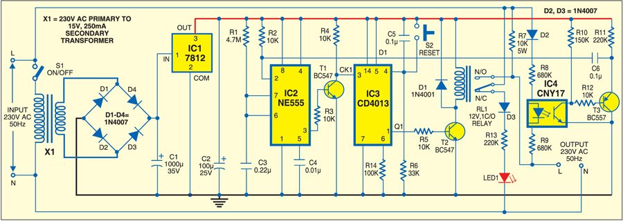
The switch that controls the socket may also get damaged by this spark if the socket was initially turned off when the SMPS was plugged in. This reduces the lifetime of both the socket switch and the SMPS plug.

The circuit given here avoids the damage by stopping fast charging of the capacitor inside the SMPS device through a resistor.
After a delay of about one second provided by monostable IC NE555 (IC2), the capacitor inside the SMPS charges. The relay energises, closing the contact and shorting the series resistor. As the power to the SMPS is applied after some delay, the capacitor gets sufficient time to charge and thus sparking is avoided. For normal operation, first press the reset switch (S2) and then plug the SMPS to L and N terminals (refer Fig. 1).

CD4013 (IC3) is a dual D-type flip-flop. Out of the two flip-flops, only one is used here. The flip-flop is clocked by the pulse provided by timer IC2, which is configured as a monostable multi-vibrator.
When the circuit is switched on using power switch S1, IC1 provides clock pulse to the flip-flop. The Q1 output of IC3 goes high and the relay-driver transistor conducts to energise the relay. The relay remains energised until it is reset by switch S2.
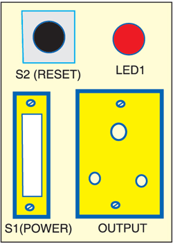
Assemble the circuit on a general-purpose PCB and enclose in a suitable case. The proposed socket arrangement is shown in Fig. 2.
