


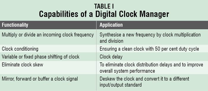
The focus in this article is on clock management in field-programmable gate arrays (FPGAs). It talks about the digital clock manager (DCM), which is a primitive used in FPGAs from Xilinx for dealing with all aspects of clock management. DCMs are used to implement delay-locked loop (DLL), digital frequency synthesiser, digital phase shifter (PS) and digital spread spectrum. They provide advanced clocking capabilities to multiply or divide the incoming clock frequency to synthesise a new clock frequency. They also eliminate clock skew, thereby improving system performance, and are capable of phase shifting the output clock to delay the incoming clock by a fraction of clock period. Table I lists the advanced clocking capabilities of a DCM.
What is DCM
Fig. 1 shows the functional block diagram of a DCM. As shown in the figure, it comprises four different functional units, namely, DLL, digital frequency synthesiser (DFS), PS and status logic (SL).
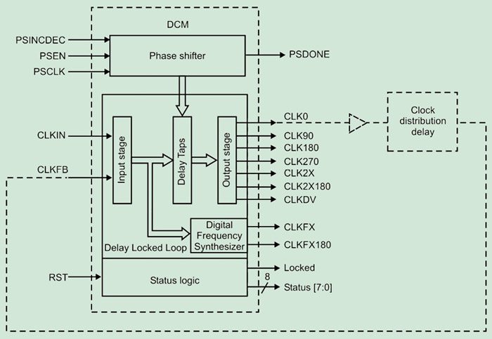

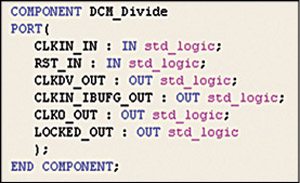
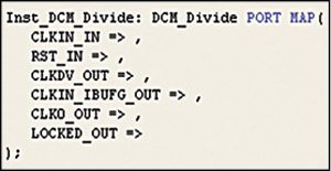
The DLL unit provides an on-chip digital deskew circuit that generates output clock signals having zero propagation delay. The input signals to the DLL unit are CLKIN and CLKFB. The output signals from the DLL are CLK0, CLK90, CLK180, CLK270, CLK2X, CLK2X180 and CLKDV. The deskew circuit compensates for the delay on the routing network by monitoring the output clock (either the CLK0 or the CLK2X).
The DFS unit provides a wide and flexible range of output frequencies based on the ratio of two user-defined integers, a multiplier (CLKFX_MULTIPLY) and a divisor (CLKFX_DIVIDE). The output frequency is derived from the input clock (CLKIN) by simultaneous frequency division and multiplication.

The PS unit controls the phase relations of the DCM’s clock outputs with respect to the CLKIN input. It shifts the phase of all nine DCM clock output signals by a fixed fraction of the input clock period. The fixed phase-shift value is set at design time and loaded into the DCM during FPGA configuration.
The PS unit also provides a digital interface for the FPGA application to dynamically advance or retard the current shift value by 1/256th of the clock period. The input signals to the PS unit are PSINCDEC, PSEN and PSCLK. The output signals are PSDONE and the STATUS[0].
The SL unit indicates the current state of the DCM via the LOCKED and STATUS[0], STATUS[1] and STATUS[2] output signals. The LOCKED output signal indicates whether the DCM outputs are in phase with the CLKIN input or not. The STATUS output signals indicate the state of the DLL and PS operations. The RST input signal resets the DCM logic and returns it to its post-configuration state.
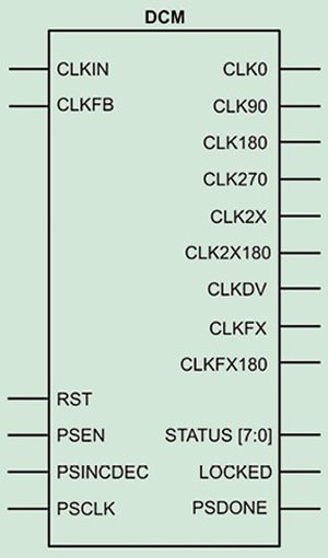
Fig. 2 shows the DCM primitive.
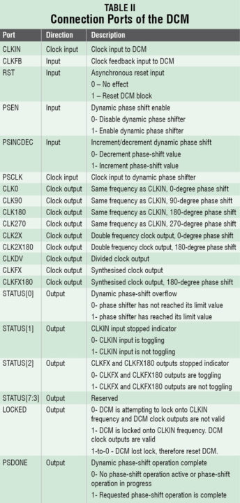
The connection ports of the DCM are described in Table II.
Using DCM
Let us see how to use the DCM wizard to configure and instantiate the DCM module.
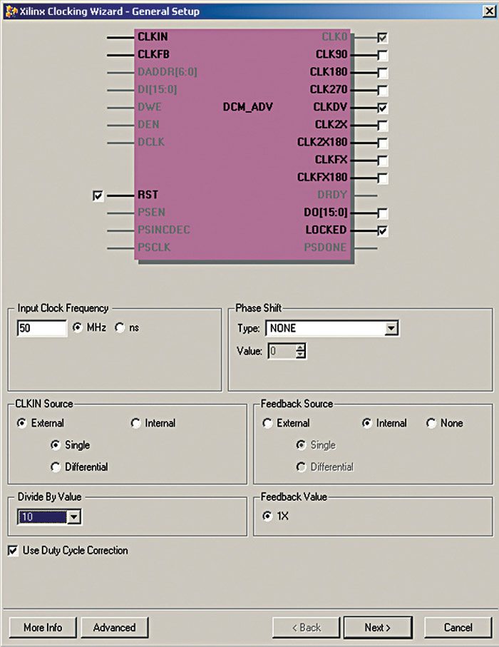
The design uses the DCM wizard to divide the input clock of 50MHz to 100kHz, which is then used to drive other circuits. One can use DCM for other applications mentioned above, including de-skewing, clock phase shifting and so on.
Steps for using the DCM wizard
1. Create an integrated software environment (ISE) project.
(i) Launch an ISE. Select Start → Programs → Xilinx ISE Design Suite 13.4_1 → ISE Design Tools → Project Navigator
(ii) In Project Navigator, select File → New Project. The new project wizard opens.
(iii) In the location option, select the folder you want to work in. (We are working in the location C:/DCM. Select C:/DCM.) Click OK.
(iv) In project name, type DCM_ClockDivider.
(v) Keep the top-level source type as HDL.
(vi) Click the Next button.
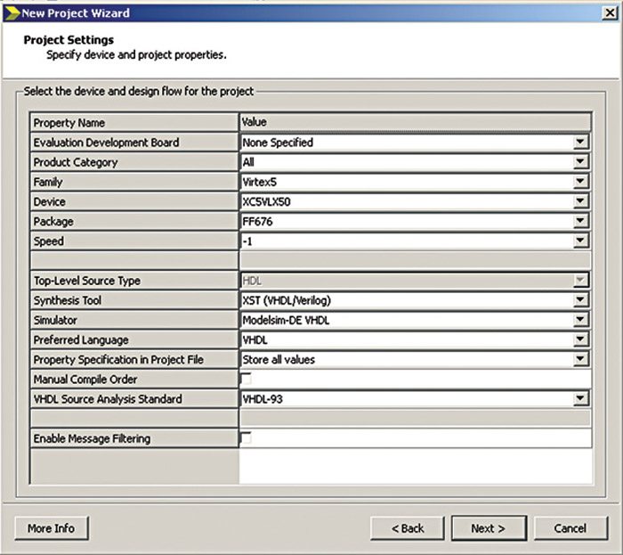
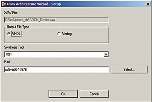
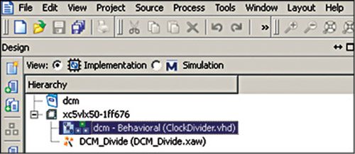
(vii) Select the family and the FPGA device type and other parameters in accordance with the FPGA and other tools you have. (We have used Virtex 5 series FPGA family, device type number XC5VLX50, package as FF676 and speed grade -1.) The project settings window looks as shown in Fig. 3.
(viii) Click Next and then Finish buttons.
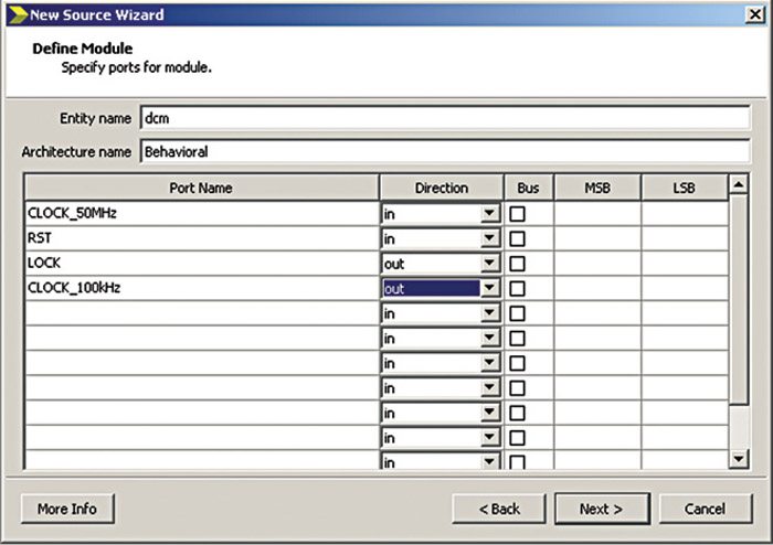
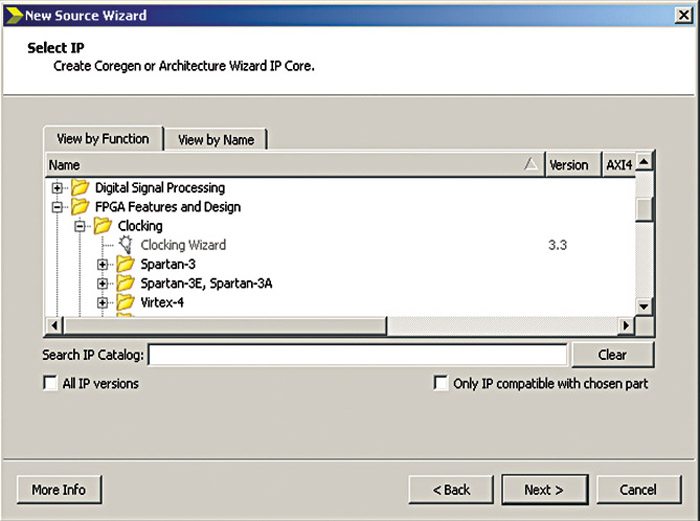
2. In the Project tab, select New Source and the New Source Wizard will appear.
3. Select VHDL module and type ClockDivider in the File name field.
4. Check if Add to Project option is ticked. If not, tick it.
5. Click Next and I/O port of the module will be displayed in the New Source Wizard window (Fig. 4).
