


Nowadays, field programmable gate arrays (FPGAs) are widely used in a variety of embedded applications as they offer complete system solutions on a single chip including digital signal processing, data storage and processing, software-defined radio, ASIC prototyping, speech recognition, computer vision, cryptography, instrumentation, telecommunications, medical imaging, defence systems, bioinformatics, computer hardware emulation, re-configurable computing and so on. An FPGA uses an array of logic blocks, which can be configured by the user. The term ‘field programmable’ signifies that the device is programmable outside the manufacturing unit. Some of the contemporary FPGA devices offer logic complexity equivalent to that of several million system gates. Also, these devices offer features like built-in hardwired processors and related peripherals, large memory, clock management systems and support for many of the contemporary device-to-device signalling technologies.
In a nutshell, FPGAs are central to any modern electronic system design. FPGAs form a customisable chip flexible enough to be deployed in a wide range of applications. They are the backbone of many complex ‘system-on-chip’ designs.

Designers and application engineers are always in need of a ready reference that provides them all the critical information for their day-to-day work. This series of articles is written with an aim to help them interface FPGA with the real-world devices. This is the first part in the series, which gives a brief overview of FPGA essentials in terms of fundamental concepts and other practical information. This is followed by ready-to-use guidelines for designing I2C (inter-integrated circuit bus) master controller in an FPGA. The format of each article in the series is such that it provides the introduction to the topic, hardware connection details and VHDL code listing and description. Attempt is made to provide all details related to the topic so as to make the article a complete capsule in itself.

Introduction to FPGA
Internal architecture of an FPGA device has three main parts, namely, array of logic blocks, programmable interconnects and I/O blocks. Fig. 1 shows the architecture of a typical FPGA. Each of the I/O blocks provides individually selectable input, output or bidirectional access to one of the general-purpose I/O pins on the FPGA package. Logic blocks in an FPGA are no more complex than a couple of logic gates or a look-up table feeding a flip-flop. Programmable interconnects not only connect logic blocks to logic blocks but also connect I/O blocks to logic blocks.
Major manufacturers of FPGA devices include Xilinx, Altera, Lattice Semiconductor, MicroSemi (Actel) and SiliconBlue Technologies. Out of these, Xilinx and Altera are the market leaders and manufacture 80 per cent of the FPGAs used in the industry. Xilinx offers Xilinx 7 series (Virtex-7, Kintex-7, Artix-7) based on the 28nm HPL process technology, Zynq-7000 family which integrates an ARM Cortex-A9 MPCore processor on 28nm FPGA, Virtex series and Spartan series of FPGAs. Altera offers the Stratix, Arria and Cyclone series of FPGAs.

Details of I²C protocol, hardware connection and VHDL code are presented in the following sections.
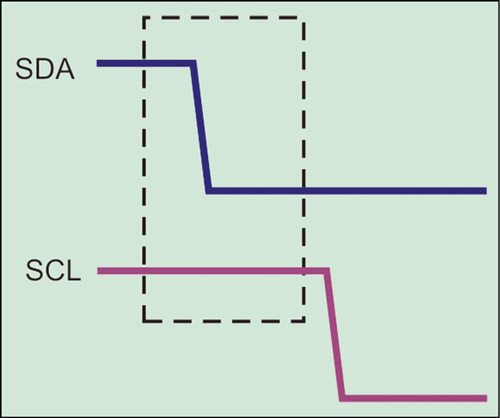
I²C protocol
I²C is a simple bi-directional serial bus, which supports multiple masters and slaves. The I²C protocol was developed by Philips in 1982 to reduce the connection pin count. It comprises a serial bi-directional data line (SDA) and a serial bi-directional clock line (SCL). Both these lines are open drained. SDA must be pulled up to VCC with a 5.6-kilo-ohm resistor and SCL also needs to be pulled up with the same resistor only if there are multiple masters in the system or when the slave will perform clock stretching as a flow control measure to synchronise with the master. I2C bus supports various modes, namely, the slow-speed mode (maximum speed of 10kbps), standard mode (maximum speed of 100kbps), fast mode (maximum speed of 400kbps), fast mode plus (maximum speed of 1Mbps) and high-speed mode (maximum speed of 3.4Mbps).

Why do the state seem to be random numbers? Also, why use such a large data type for the states if only 17 states are required?