VHDL code listing
The process flow followed to drive the LCD is as follows:
1. Write 0×38, wait 4.2 milliseconds
2. Write 0×38, wait 4.2 milliseconds
3. Write 0×38, wait 4.2 milliseconds
4. Write 0×38, wait 4.2 milliseconds (function set, two-line display and 5×8 dot character font)
5. Write 0×08, wait 4.2 milliseconds (display off, cursor off)
6. Write 0×01, wait 4.2 milliseconds (display clear)
7. Write 0×0C, wait 4.2 milliseconds (display on, cursor off)
8. Write 0×06, wait for 4.2 milliseconds (shift cursor to right)
9. Write ASCII ‘W’, wait 4.2 milliseconds
10. Write ASCII ‘E’, wait 4.2 milliseconds
11. Write ASCII ‘L’, wait 4.2 milliseconds
12. Write ASCII ‘C’, wait 4.2 milliseconds
13. Write ASCII ‘O’, wait 4.2 milliseconds
14. Write ASCII ‘M’, wait 4.2 milliseconds
15. Write ASCII ‘E’, wait 4.2 milliseconds
As shown in the flowchart in Fig. 6, all steps do not require a few milliseconds for execution. However, to simplify the code, the time for all the steps is kept uniform. In case this is found unsuitable for the design, the designer can modify the timings.
Instead of using delays, one can check the status of the busy flag to see if the LCD is ready to receive information. The busy flag is the MSB of the data bus and can be read when R/W = 1, RS = 0 and low-to-high pulse is applied to the EN pin. If the busy flag is high, the LCD is busy taking care of the internal operations and will not accept any new information. When the busy flag is low, the LCD is ready to accept new information.

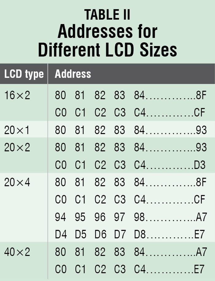
The VHDL code (LCD_fpga.vhd) for implementing the LCD controller is included in this month’s EFY DVD. The code writes ‘WELCOME’ on the LCD display. The LCD display used here is 16×2. One can use any display and change the initialisation commands accordingly.
VHDL code description

 The code begins with the standard library to be included. The ENTITY section defines the interface between the LCD module and the outside world. It includes all the input and the output connections including the 50MHz clock (Clock) and reset (Reset) as inputs, LCD register select (LCD_RS) and LCD enable (LCD_E) as outputs, LCD read/write (LCD_RW) as buffer and 8-bit data bus (DATA_BUS) as inout. DATA_BUS is defined as inout so that it is capable for both input and output operations.
The architecture section defines the two operations of the LCD module for generating the LCD clock and implementing the FSM. The different signals defined in the architecture include state and next_command of state_type, DATA_BUS_VALUE which is an 8-bit STD_LOGIC_VECTOR, COUNT_CLK_LCD which is a 28-bit STD_LOGIC_VECTOR and CLK_LCD which is a STD_LOGIC signal. The value of the signal DATA_BUS_VALUE is ported to port DATA_BUS when LCD_RW is at logic ‘0’, otherwise the port DATA_BUS remains in the high-impedance state.
The state_type is a signal type that defines different states of the LCD, namely Hold, Display_ON, Mode_SET, Write_CHAR1, Write_CHAR2, Write_CHAR3, Write_CHAR4, Write_CHAR5, Write_CHAR6, Write_CHAR7, Return_HOME, Toggle_E, Reset1, Reset2, Reset3, Display_OFF and Display_CLR. The state and next_command are two signals of state_type.
As mentioned before, the first operation generates the slow clock for the LCD. It uses the 21st bit of the COUNT_CLK_LCD signal; the clock signal for the LCD is named as CLK_LCD.
The second operation is the FSM that drives the LCD. If the Reset pin is in high state, the LCD is initialised by sending 0×38 in hex on the data bus. RW and RS signals are set to ‘0’ and the Enable pin is set to ‘1.’ The current state is defined as Reset1 and the next_command state as Reset2. When the Reset pin is in low state, the FSM of driving the LCD is implemented. The different states of the FSM are Reset1, Reset2, Reset3, Display_OFF, Display_CLR, Display_ON, Mode_SET, Write_CHAR1, Write_CHAR2, Write_CHAR3, Write_CHAR4, Write_CHAR5, Write_CHAR6, Write_CHAR7 and Return_HOME. Toggle_E and Hold are two sub-states.
For LCD initialisation, the command ‘0×38’ (hex) is sent to LCD in three states: Reset1, Reset2 and Reset3. It may be mentioned here that the command is dependent on the size of the LCD being used. The ‘0×38’ is used to initialise a 16×2 LCD. The RS and RW signals are set at logic ‘0.’ Enable signal is set at logic ‘1.’ The FSM is directed to sub-state Toggle_E where the Enable signal is made to go to logic ‘0’ and the FSM is directed to the Hold sub-state. The Hold sub-state directs the FSM to the next state next_command as set in the main states earlier. Remember that the data on the data bus is latched by the LCD on the high-to-low transition of the Enable signal.