


Presented here is a FIFO design using Verilog that is simulated using ModelSim software. In this article, we design and analyse FIFO using different read and write logics. We have considered 64 inputs, each having 32-bit data.
FIFO design
FIFO is an approach for handling program work requests from queues or stacks so that the oldest request is handled first. In hardware, it is either an array of flops or read/write memory that stores data from one clock domain and on request supplies the same data to other clock domains following FIFO logic.
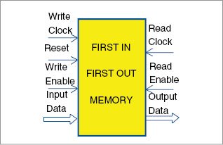
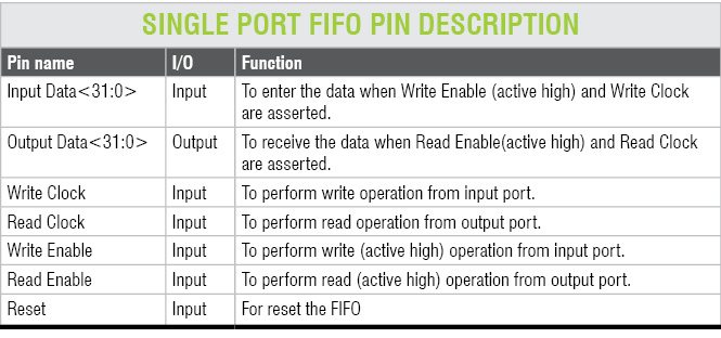
Clock domain that supplies data to FIFO is often referred to as write or input logic, and clock domain that reads data from FIFO is often referred to as read or output logic. Pin diagram of FIFO is shown in Fig. 1 and its description in the table.

FIFOs are used in designs to safely pass multi-bit data words from one clock domain to another, or to control the flow of data between source and destination sides sitting in the same clock domain. If read and write clock domains are governed by the same clock signal, FIFO is said to be synchronous. If these are governed by different (asynchronous) clock signals, FIFO is said to be asynchronous. A synchronous FIFO example is described here.
Input port is controlled by write-clock and write-enable inputs. Data is written into FIFO on every rising edge when it is asserted. Output port is controlled by read-clock and read-enable inputs. Data is read from FIFO on every rising edge and read-enable is asserted.

Software program
Verilog has been used for register-transfer logic (RTL) coding and verification. The bottom-up design has been followed in this article in order to facilitate easy debugging of the various modules.
ModelSim is an easy-to-use yet versatile VHDL/SystemVerilog/Verilog/SystemC simulator from Mentor Graphics. It supports behavioural, register-transfer-level and gate-level modelling.
To start FIFO design simulation, install ModelSim V10.4a on a Windows PC and follow the steps mentioned below.
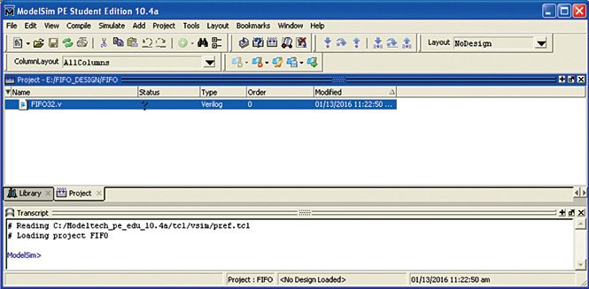
1. Start ModelSim from the desktop; you will see ModelSim 10.4a dialogue window.
2. Create a project by clicking Jump Start on Welcome screen.
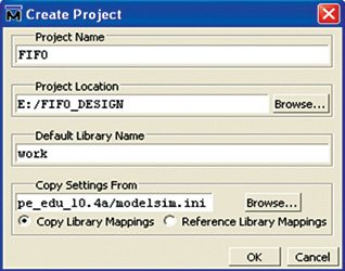
3. Create Project window pops up (Fig. 2). Select a suitable name for your project. Set Project Location to E:\FIFO_DESIGN (in our case) and leave the rest as default, followed by clicking OK.
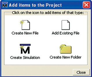
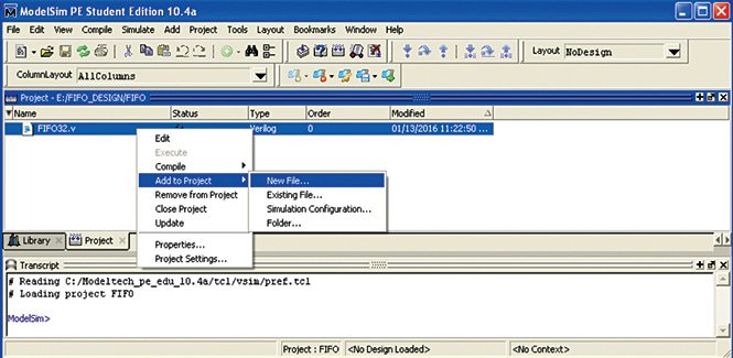
4. Add items to the Project window pops up (Fig. 3).
5. On this window, select Create New File option.
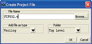
6. Create Project File window pops up. Give an appropriate file name (say, FIFO32.v) for the file you want to add, and choose Verilog as Add file as type and Top Level as Folder (Fig. 4).
7. On the workspace section of the main window (Fig. 5), double-click on the file you have just created (FIFO32.v in our case).
8. Type your Verilog code (FIFO32.v) in the new window. Since we have considered 64 inputs, first data being 32’ h42_41_4C_4C and last being 32’h41_52_54_49, our main goal is to verify that first data comes out in the simulation output window. Note that these inputs are arbitrary and so you can enter any 32-bit data.
9. Save your code from File menu.
10. Add relevant source files that form the internal architecture of FIFO. These include D-Flipflop, 2-bit mux, Basic cell, 32-bit word, core and so on. Add new files to FIFO project by right-clicking FIFO32.v file. Select Add to Project→New File options as shown in Fig. 6.
Give File Name mux21 and follow the steps from 7 through 9 as mentioned above.
Similarly, add other files to the project and enter respective Verilog codes in these files.
Details of this FIFO can be obtained from the relevant source files, which are sub modules of FIFO.
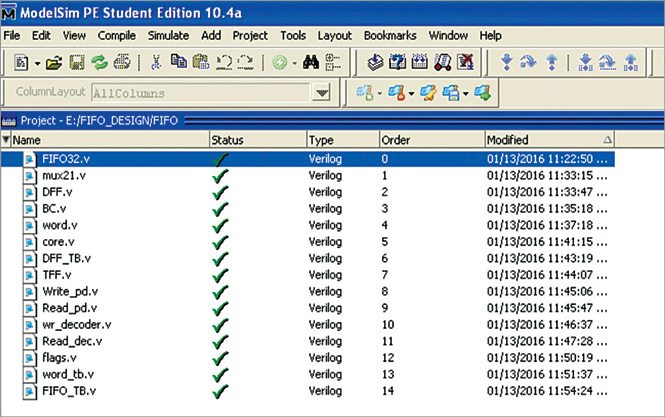
The final workspace window is shown in Fig. 7.
Compiling/debugging project files
1. Select Compile→Compile All options.
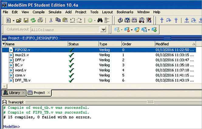
2. The compilation result is shown on the main window. A green tick is shown against each file name, which means there are no errors in the project (Fig. 8).
Download source code: click here
Simulating FIFO design
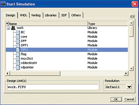
1. Click on Library menu from the main window and then click on plus (+) sign next to the work library. You should see the name FIFO that we have just compiled (Fig. 9).
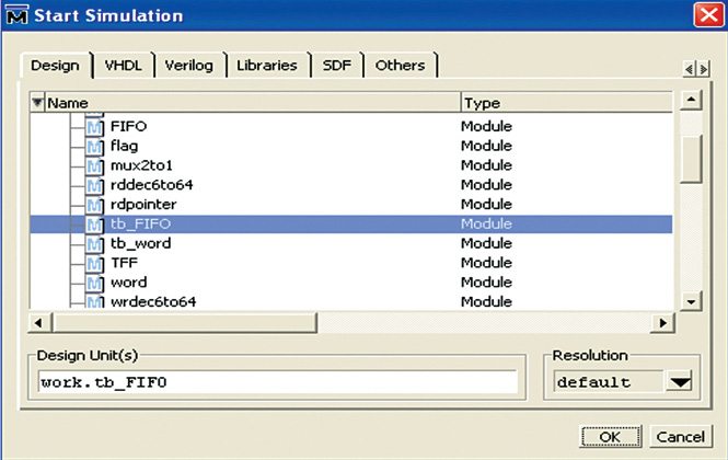
2. Now in work library, select tb_FIFO and click on OK (Fig. 10). This will open sim-Default window as shown in Fig. 11.
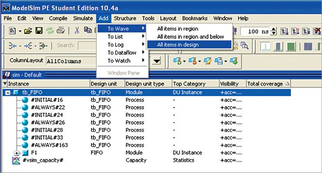
3. Go to Add→To Wave→All items in design options.
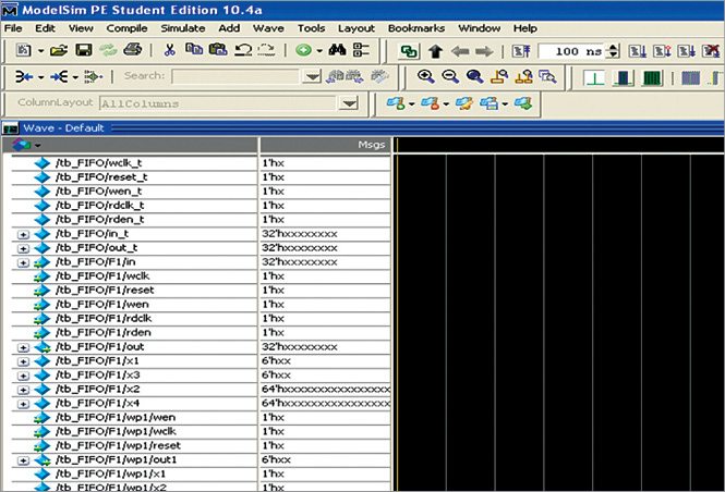
4. Select the signals that you want to monitor for simulation purposes. Select these as shown in Fig. 12.
5. Selected signals are the test bench to verify FIFO functional behavior. We are now ready to simulate our design by clicking Run from Simulate menu bar as shown in Fig. 13.
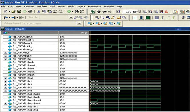
Now, click on Zoom Full from Wave window. Your simulation output waveform will be as shown in Fig. 14. Note that, we have already provided 32-bit input values to all 64 address locations. You can check the first data as 32’ h42_41_4C_4C in the first location on this screenshot. By scrolling the cursor towards right, you can see the data in the last location as 32’h41_52_54_49.
Thus, the result of FIFO design is verified from this output waveform.
Future applications
FIFO logic described here can be further refined to make more advanced-level projects. For example, in system on chip designs, there are components that often run on different clocks. So to pass data from one component to another, we need an asynchronous FIFO.
Sometimes, even if the source and request sides are controlled by the same clock signal, FIFO is needed. This is to match the throughputs of the source to the request. For example, the source may be supplying data at the rate at which the request cannot handle or, in other case, may be placing requests for data at a rate at which source cannot supply. Here, a synchronous FIFO is used that acts as an elastic buffer.
Feel interested? Check out other projects in the circuit section.


i have some questions about the project description, can i list my questions or is there a description for the code?
Please email your queries to abhimanyu.rathore@efy.in.