


Stop clock is widely used in various fields to measure the timing of events. Science laboratory experiments, such as measurement of discharge rate of capacitors with different resistors, acceleration due to gravity and velocity of an object, require an accurate stop clock. Also, in sports almost all the track events need such a clock to measure the timings.
Presented here is a stop clock built with a basic AT89C52 microcontroller that can be used in a variety of fields to measure events. This construction project can also help you understand concepts like real-time use of microcontrollers and scanning related to displays. The device is dual powered and will switch to battery supply if mains is ‘off.’
Circuit and working
Fig. 1 shows the circuit of stop clock. In addition to microcontroller AT89C52 (IC1), the stop clock requires use of seven-segment displays LTS542 (DIS1 through DIS6), regulator 7805 (IC2) and a few discrete components.


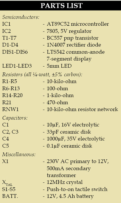 IC1 is a low-power, high-performance CMOS 8-bit microcontroller. It has 8 kB of Flash, 256 bytes of RAM, 32 input/output (I/O) lines, three 16-bit timers/counters, a six-vector two-level interrupt architecture, a full-duplex serial port, on-chip oscillator and clock circuitry. The microcontroller has four I/O ports. Here ports P0 and P2 are used to drive seven-segment displays (DIS1 through DIS6) and LEDs (LED1 and LED2).
Port pins P2.0 through P2.7 of IC1 are connected to seven-segment displays as shown in Fig. 1. To make the PCB layout easier, DIS1, DIS3 and DIS5 are connected differently than DIS2, DIS4 and DIS6. Pins e, d, c, dp, b, a, f and g of 7-segment displays DIS1, DIS3 and DIS5 are connected to port pins P2.0 through P2.7, respectively, whereas in case of DIS2, DIS4 and DIS6, pins dp, c, d, e, g, f, a and b are connected to port pins P2.0 through P2.7, respectively. This is actually a trade-off as simplicity of the PCB layout has increased the complexity of the scanning software.

Port P2 provides segment data for 7-segment displays DIS1 through DIS6. Port pins P0.1 through P0.7 of IC1 are pulled up with a 10-kilo-ohm resistor network (RNW1). P0.2 through P0.7 are used to select the seven-segment displays. These pins drive the base of pnp transistors T7 through T2 to select the corresponding display. For example, if pin P0.2 of microcontroller AT89C52 goes low, transistor T7 is driven into saturation, which provides supply to the common-anode pin 3 or pin 8 of 7-segment display DIS6.
Microcontroller IC1 provides segment data and display-enabled signal simultaneously in time-division multiplexing mode for displaying a particular number on the seven-segment display. Segment data and display-enabled pulse for the display are refreshed continuously at a very fast rate. Thus the display appears to be continuous due to persistence of vision even though the segment displays light up one by one. Port pin P0.1 is used to drive LED1 and LED2 so as to provide dots between DIS2 and DIS3, and DIS4 and DIS5, respectively.
Switches S1 through S4 are used for reset, start, stop and load. Port pins P3.0 through P3.3 are pulled up by resistors R1 through R4 and connected to switches S1 through S4, respectively. Switch S5 is used to manually reset the microcontroller, while the power-‘on’ reset signal for the microcontroller is derived from the combination of capacitor C1 and resistor R5. A 12MHz crystal is used to generate clock frequency for the microcontroller.
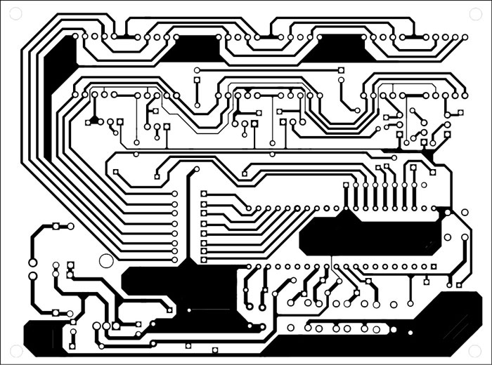
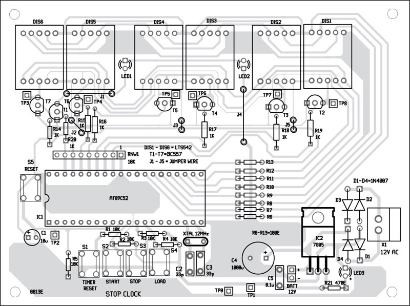
Download PCB and Component Layout PDFs: Click here
Fig. 2 shows the power supply circuit. The 230V, 50Hz AC mains is stepped down by transformer X1 to deliver a secondary output of 12 V, 500 mA. The transformer output is rectified by a full-wave bridge rectifier comprising diodes D1 through D4, filtered by capacitor C4 and regulated by IC 7805 (IC2). Capacitor C5 by-passes ripples present in the regulated output. LED3 acts as the power indicator. Resistor R21 acts as the current limiter for LED3. A rechargeable battery (BATT.) is used for power backup.
Working of the project is simple. When power is switched on, it displays ‘00.00.00,’ and both LEDs (LED1 and LED2) are ‘off.’
The stop-clock can display minutes, seconds and centi-seconds, and both the LEDs remain ‘off’ up to one hour. After one hour, the centi-seconds disappear and both the LEDs glow to indicate that the reading is in hours.
The functions of all the four switches are as follows:
Reset (S1): Reset the stop clock at any time (whether the stop clock is running or stopped)
Start (S2): Start the stop clock again
Stop (S3): Stop the stop clock
Load (S4): Record the timings when the clock is running. The recorded reading can be seen after pressing ‘Stop.’


can you explain details…Tp3 to Tp8