


 This project controls home electrical appliances using a touchscreen input device. The system comprises two relays for controlling a bulb and a fan as an example. The touchscreen placed on a graphical LCD acts as a control panel for sending control commands through a pair of wireless radio frequency (RF) communication modules. The touchscreen panel on the transmitter side interfaced to a microcontroller sends on/off commands to the receiver where the loads/appliances are connected. By touching the specified portion on the touchscreen panel, the loads are turned on/off remotely through the wireless RF modules.
Circuit and working
The system is divided into transmitter and receiver sections.
Transmitter section
Block diagram of the transmitter section is shown in Fig. 1. The power supply unit is used to power the microcontroller, RF Tx module and graphics LCD (GLCD)

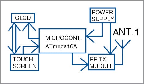
The GLCD is interfaced with the microcontroller. The touchscreen is transparent and is hence placed on top of the GLCD. Data obtained from the touchscreen is processed by the microcontroller to generate a 4-digit binary code. This code is encoded by the encoder and transmitted through the RF transmitter and antenna.
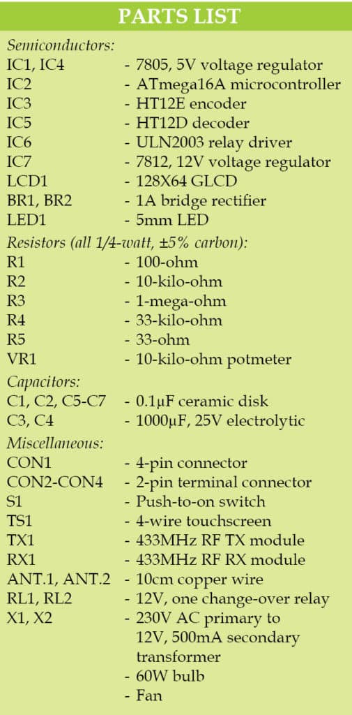
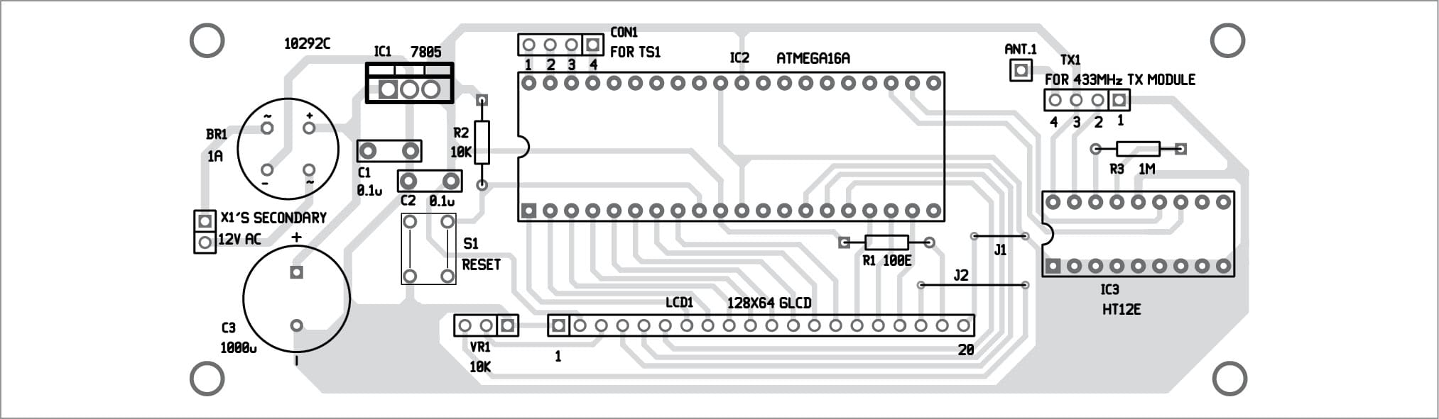
Circuit diagram of the transmitter section is shown in Fig. 2. It is built around transformer X1, bridge rectifier BR1, 128×64 GLCD (LCD1), 4-wire touchscreen (TS1), 5V voltage regulator 7805 (IC1), ATmega16A microcontroller (IC2), encoder HT12E (IC3), 433MHz RF transmitter module (TX1), an antenna (ANT.1) and a few other components.

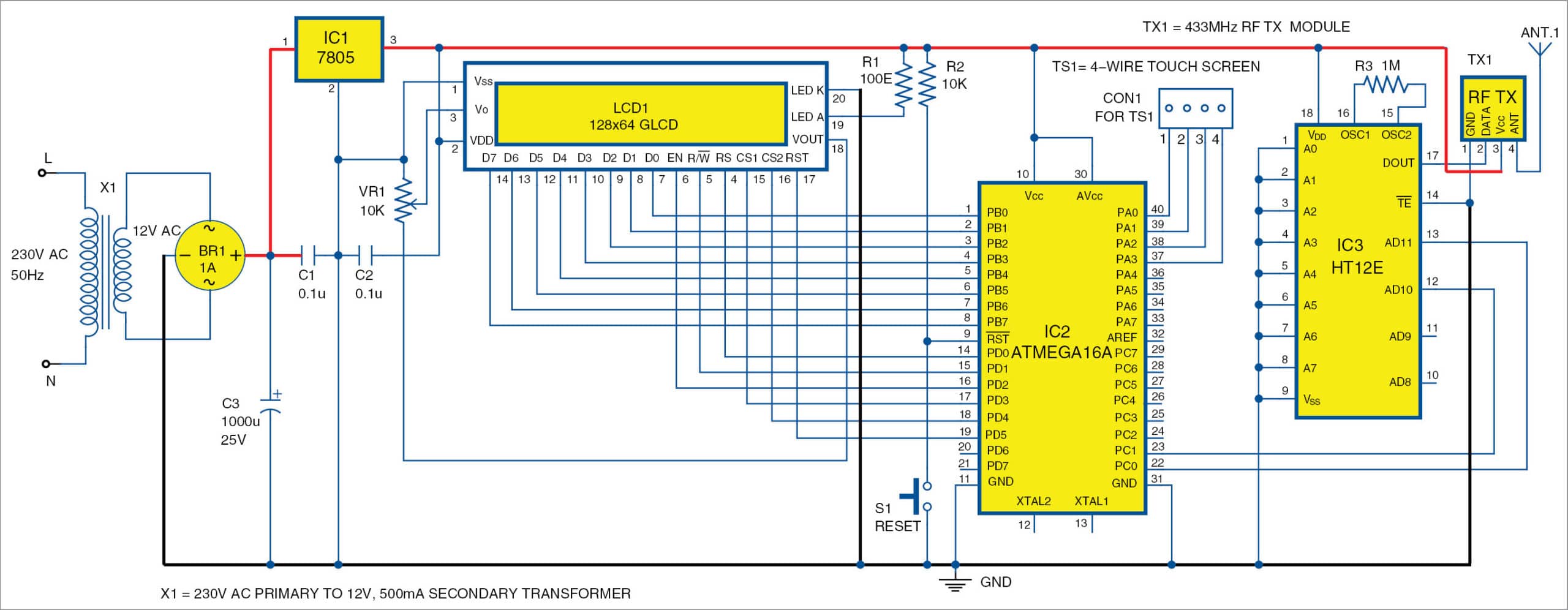
TS1 is connected directly to the microcontroller. The touchscreen has four wires, namely, X+, X-, Y+ and Y-. All these wires are connected to four analogue-to-digital converter (ADC) pins of Port A of IC2. Wire X+ (pin 1) is connected to PA0, X- (pin 2) to PA1, Y+ (pin 3) to PA2 and Y- (pin 4) to PA3.
Data pins D0 through D7 of GLCD are connected to Port B pin PB0 through PB7 of ATmega16A, respectively. As 1MHz internal clock of ATmega16A is used, there is no need for an external crystal. RST pin 9 of IC2 is connected to ground through switch S1.
On pressing S1 momentarily, IC2 will get reset. Control pins (RS, R/W, EN, etc) of the GLCD are connected to Port D of ATmega16A. There are two chips in GLCD that are controlled by control pins CS1 (pin 15) and CS2 (pin 16) connected to pins 17 and 18 of IC2, respectively. The reset pin (RST) of the GLCD (pin 17) is connected to pin 19 of IC2.
Since output of the touchscreen is analogue, the user needs to convert it into digital. This is done by the internal ADC of ATmega16A. Port A has an inbuilt ADC, so an external ADC chip (like ADC 0804) is not required.
Ports PC0 and PC1 of IC2 are connected to encoder IC3. All addresses from A0 to A7 of encoder IC3 and decoder IC5 are connected to ground in both transmitter and receiver circuits. For transmission, TE pin (pin 14) of IC3 is connected to ground. The output (DOUT) of IC3 is connected to data pin 2 of TX1 to transmit the bits through RF signals.
Working of the transmitter section is simple. When the user touches ‘light on’ symbol on the touchscreen, resistance of the touchscreen changes, and it changes the voltage across the touchscreen output. This voltage difference is converted to a digital signal by the ADC of ATmega16 microcontroller. ATmega16A checks the X and Y co-ordinates range. If it is in the predefined range, it sets the output according to the user’s requirement at Port C. This signal is transmitted using 433MHz RF Tx module through an antenna (ANT.1).
Receiver section
Block diagram of the receiver section is shown in Fig. 3. The power supply unit is used to power the decoder and RF receiver module. The four-digit binary codes transmitted through the transmitter section are received by ANT.2 of the receiver circuit.
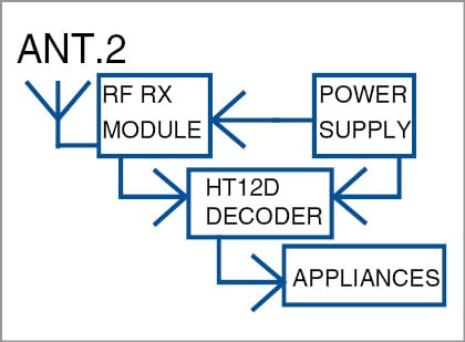
Here, the decoder is used to decode the received signal. The microcontroller in the transmitter section switches the devices/appliances connected to the receiver section accordingly.
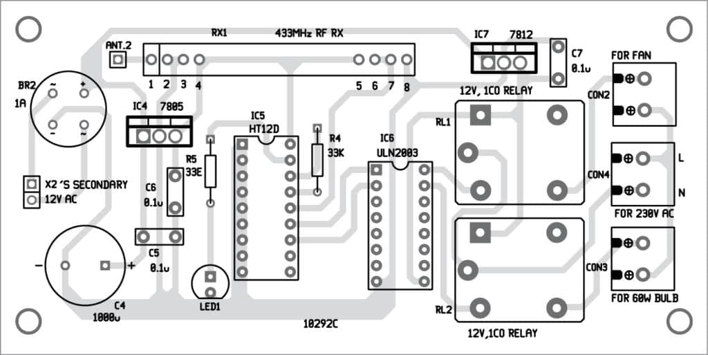
Circuit diagram of the receiver section is shown in Fig. 4. It is built around transformer X2, bridge rectifier BR2, 5V voltage regulator 7805 (IC4), decoder HT12D (IC5), 433MHz RF receiver module (RX1), an antenna (ANT.2), relay driver ULN2003 (IC6), 12V voltage regulator 7812 (IC7), two 12V, single-changeover relays (RL1 and RL2) and a few other components.

In the receiver section, data pins of RX1 are connected to DIN (pin 14) of decoder HT12D (IC5). All address pins of IC5 are connected to ground as in IC3 in transmitter section. Two output pins (D10 and D11) of IC5 are connected to two input pins IN1 (pin 1) and IN2 (pin 2) of ULN 2003 (IC6). Output pins 16 and 15 of IC6 are connected to relays RL1 and RL2, respectively. Two voltage regulators (5V and 12V) are used here, 5V for the circuit and 12V for the relays.
Working of the receiver section is simple. When the user touches ‘light on’ symbol on the touchscreen at the transmitter side, data in the form of 1s and 0s is transmitted through ANT.1 and reaches the receiver through ANT. 2. This data reaches decoder IC5 through 433MHz RF Rx module. IC5 decodes the data and output to IC6. Respective relays are energised through IC6. The appliances are switched on through the contacts of the respective relays.
If the user touches ‘light off’ symbol on the touchscreen, D10 output of IC5 becomes low. This low output is applied to pin 2 (IN2) of IC6, causing pin 15 (OUT2) to become high. This de-energises relay RL2, and the bulb is turned off. Similar is the case with the fan.
Software
The code is written in C programming language for the AVR and compiled in Atmel Studio 6.2. The program is uploaded to the microcontroller using STK500. ProgISP programmer was used to burn the hex code at EFY Lab. Before uploading the hex code (touchscreen.hex), set the following fuse bits:
LOW = C1
HIGH = 99
Download Source Code
Construction and testing
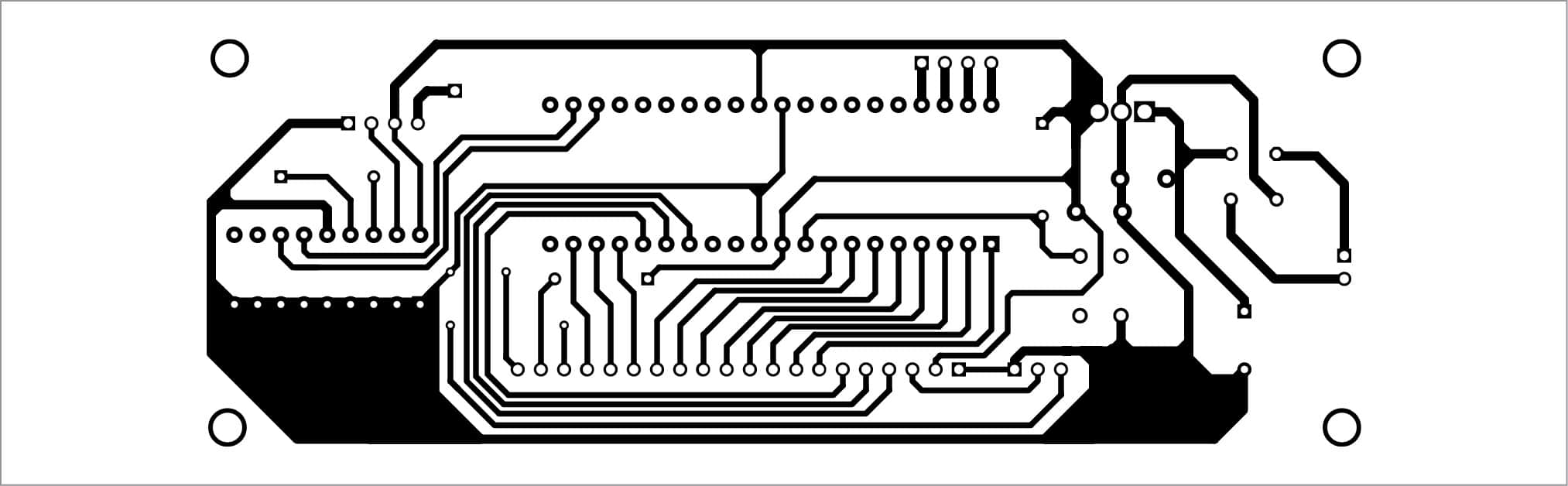
An actual-size PCB layout for the transmitter section is shown in Fig. 5 and its components layout in Fig. 6. Assemble the components—including the touchscreen, GLCD, ANT.1 and TX1—on the PCB. Note that only secondary terminals of X1 (12V AC) are shown in the PCB. Place X1 at a suitable location inside the enclosure.
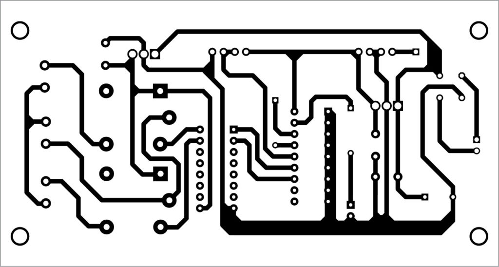
An actual-size PCB layout for receiver section is shown in Fig. 7 and its components layout in Fig. 8. Assemble the components on the PCB. Connect the secondary terminals of X2 (12V AC) to the PCB.
Download PCB and component layout PDFs: click here
After loading the code, insert IC2 into the PCB. Place the receiver unit at a distance of about 10 to 30 metres away from the transmitter. Connect the two appliances across RL1 and RL2 in the receiver unit. Connect power supplies to the transmitter and receiver circuits. Now the user can touch the symbols on the touchscreen in the transmitter unit to switch on/off the appliances.

can i have the source code?
Kindly refresh the page and redownload from the Source code download button from the article.