 A logic probe is a handheld pen-like probe used for analysing and troubleshooting the logical states ‘0’ or ‘1’ of a digital circuit. While most logic probes are powered by the circuit under test, some probes use batteries. These can be used for either TTL (transistor-transistor logic) or CMOS (complementary metallic oxide semiconductor) integrated circuit devices. The circuit described here can be used for TTL logic only, and shows the presence of either state (logic 1 or 0).
As shown in Fig. 1, the logic probe circuit is built around four transistors and a few passive components. It uses two LEDs that show logic states 1 (green) and 0 (red). The green LED glows when the voltage at probe tip exceeds about 2.4V and the red LED glows when this voltage falls below about 1.2V, which is adequate to detect the normal TTL levels. When no LED glows, it means the probe is in suspended state, i.e., it is neither showing logic 1, nor logic 0.
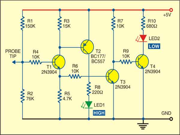
Working of the logic probe circuit is simple and can be divided into three states: The probe is suspended, the probe’s tip is at logic 1 and the probe’s tip is at logic 0.When the probe is in suspended condition, the junction voltage of resistors R1 and R2 is almost equal to that obtained when R1 and R2 alone form a voltage divider bias for the supply voltage. Under this condition, the base-emitter junction of transistor T1 is forward biased, so the voltage drop across resistor R5 (>0.6V) is enough to drive transistor T3 into conduction, which, in turn, cuts off transistor T4. As a result, the red LED (LED2) does not glow. The current flowing through R3 is nearly equal to that through R5. However, this does not produce enough voltage drop (0.3V-0.6V) across resistor R3 to make transistor T2 conduct. As a result, the green LED (LED1) does not glow. Thus neither of the LEDs glows when the probe is in suspended condition.

When the probe tip is at logic 1, transistor T3 forward biases to cut-off transistor T4. But, this voltage should exceed 2.4V (normally TTL logic 1 is well above this voltage), this will cause a greater current to flow through emitter resistor R5 of T1, which also flows through collector resistor R3 causing a larger voltage drop across R3. Thus transistor T2 conducts and the green LED (LED1) glows to indicate the presence of logic 1 (high) at the probe tip.
When the probe tip is at logic 0, transistor T3 cuts off to make transistor T4 conduct. As a result, the red LED (LED2) glows to indicate logic 0 (low). It can be easily seen from the circuit diagram that a voltage of more than 1.2 volts is required at the probe tip to forward-bias transistors T1 and T3 whose base-emitter junctions appear in series in the circuit. Any voltage less than this at the probe tip will not forward-bias T3, resulting in the red LED (LED1) glowing.
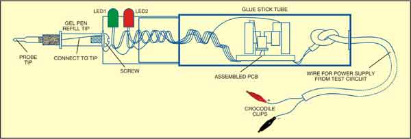
Assemble the circuit on a general-purpose PCB and insert in a small plastic tube, say, a glue stick whose inner mechanism has been removed. For the probe tip, use the front portion of a gel-pen refill. The proposed arrangement for the compact logic probe is shown in Fig. 2. Before checking the logic of any circuit, connect the black clip to the ground of the circuit and the red clip to the positive terminal of the circuit.
The main feature of the circuit is that when the supply voltage is less than about 4.0V, the red LED (LED2) glows to indicate non-standard TTL voltage supply.