 Installing a doorbell in an existing building is a difficult task as it involves wiring that can look shabby if not concealed properly. Presented here is a circuit that does not require external wiring and can be placed in small enclosures. This circuit can be used as a call bell in office, too.
Circuit and working
This circuit consists of transmitter and receiver units.
Transmitter. Circuit diagram of the transmitter is shown in Fig. 1. The transmitter circuit is built around 5V voltage regulator 7805 (IC1), encoder HT12E (IC2), a DIP switch (DIP1) and a few other components. IC2 converts 12-bit (8-bit address and 4-bit data) parallel data to serial data, which is available at its DOUT pin.

DIP1 is used to set the address bit either high or low. All 4-bit data pins (AD8 through AD11) are connected to ground to reduce power consumption because 433MHz RF transmitter module (TX1) uses on-off key (OOK) modulation. When the doorbell pushbutton switch (S2) is pressed, data along with the address is sent serially through wireless transmitter module TX1.
OOK modulation is the binary form of amplitude modulation. When data being sent is low, the transmitter is fully off, suppressing the carrier. In this state TX1 consumes very low current of about 1mA.
When data being sent is high, the transmitter is fully on. In this state current consumption of TX1 is high of about 11mA with 3V power supply.
Receiver. Circuit diagram of the receiver is shown in Fig. 2. The receiver circuit is built around 5V voltage regulator 7805 (IC3), decoder HT12D (IC4), NE555 timer (IC5), melody generator UM66 (IC6), audio amplifier LM386 (IC7) and a few other components.
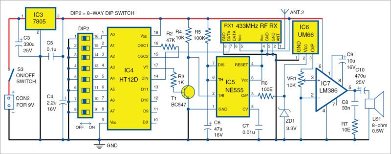
Serial data transmitted through TX1 is received by RF receiver module RX1. It is fed to pin 14 of the decoder. IC4 converts the 12-bit data into 8-bit address and 4-bit data. DIP2 is used to set the address of the decoder.
The 8-bit address of the decoder must match with the encoder to receive the information. The decoder checks the serial input three times continuously. If address bits of transmitter and receiver match, data is decoded and valid transmission VT pin of IC4 goes high. This triggers NE555 configured in monostable mode.
NE555 generates a high pulse for about five seconds, whose period is determined by resistor R5 and capacitor C6. Time period of NE555 is determined by the relationship:
Time period (in seconds) = 1.1×R5×C6
It means, when S2 is pressed momentarily, provided S1 and S3 are closed, output pin 3 of IC5 goes high for about five seconds. This output pulse activates the melody generator (IC6) and so the melody sounds up to about five seconds.
Zener diode ZD1 regulates the output of IC5 to 3.3V, which drives IC6. Output of IC6 is given to IC7 through potmeter VR1. Gain of the audio amplifier is set to 200. VR1 controls the volume of the sound before amplification.
Construction and testing
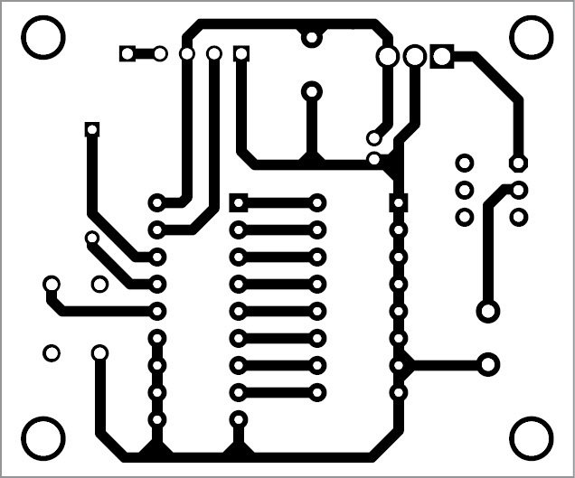
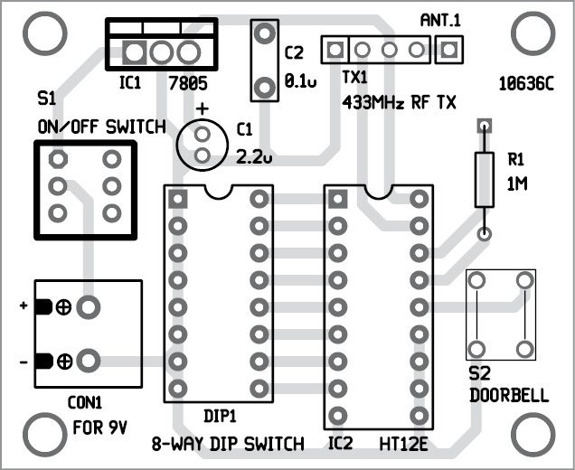
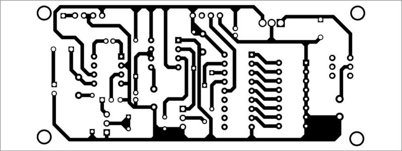
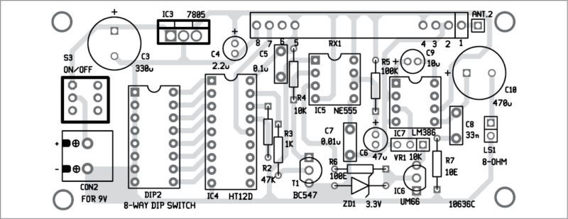
An actual-size, single-side PCB layout for the transmitter is shown in Fig. 3 and its component layout in Fig. 4. Similarly, an actual-size, single-side PCB layout for the receiver is shown in Fig. 5 and its component layout in Fig. 6.
Download PCB and component layout PDFs: click here
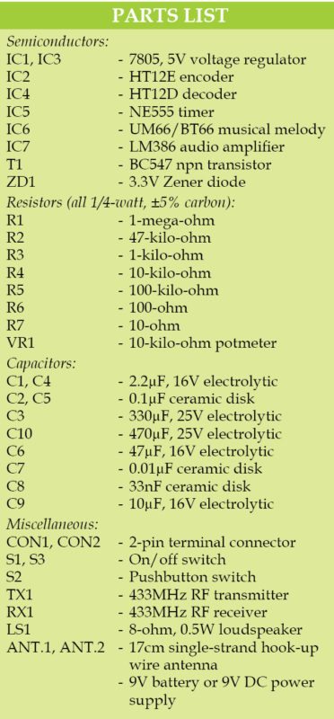
After assembling the circuits on two separate PCBs, enclose these in suitable plastic boxes. Use approximately 17cm long single-strand hook-up wire antenna for the transmitter and the receiver each. The receiver unit requires a well-regulated 9V DC power supply for low noise and efficient operation. Alternatively, a 9V battery each for the transmitter and the receiver may be used as power supplies.
We have also designed the touchless Arduino doorbell that only rings when hands are sanitized.
A. Samiuddhin is B.Tech in electrical and electronics engineering. His interests include LED lighting, power electronics, microcontrollers and Arduino programming


Thanks
You are welcome.
Thanks for wireless doorbell samiudin ji sir if you can send the circuit for led chaser that is look like running led light pl reply my cell no 9879512656
Thanks sir
You are welcome.
Dear sir I need to know how distance will it work
The range or distance depends on the RF module used. It may work from 30 meters upto 100 meters or even more…
I only have a 10w speaker
Should I make any changes or that speaker can be used too ?
In the parts list you skipped the 8 way dip switch, isn’t that necessary Sir?
You can use jumper wires in place of DIP switches DIP1 and DIP2.
The circuit is Not working.
Kindly elaborate your query.
When receiver and The Transmitter is powered The doorbell (receiver) starts to operate without pressing doorbell switch on the Transmitter circuit.
On the other hand what are the values of the resistors R7 and R6.they are not clear on the receiver circuit.
Thank you för your kind help.
Dear Sir,
I am still waiting your answer.
Thank you.
Already replied.
Problems could be wrong connection at pin 2 of NE555 or around transistor T1. Make sure that pin 2 of IC5 is high around 5V. When doorbell button S2 is pressed in transmitter side, pin 2 of IC5 should go low and you will hear the sound from speaker. You can check transistor T1 or replace it with a fresh one. The values of R6 is100-ohm and R7 is10-ohm
Very good site for for projects…..I would like to see the video of the wireless doorbell calling system please
HI Samuel, thank you for your valuable feedback. We will add Wireless Doorbell Calling System video tutorial soon.
Where can I get all the components..am in kisumu Kenya
Can I get the project report for this
from where I can get PCB and other component
Please can I get a video of how the project is done to make the project work more explanatory
Hi, thank you for your comment. We have contacted the author for sharing the video (If any) for this project.