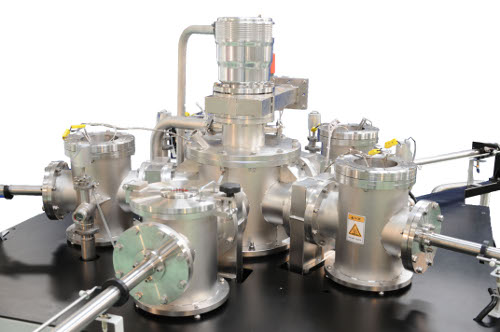
 JUNE 2012: Bengaluru-based Hind High Vacuum Co. Pvt Ltd (HHV) has recently developed a cluster-type, multi-chamber plasma–enhanced chemical vapour deposition (PECVD) system for the first time in the country, which can be used to coat different types of thin films on substrates.
HHV is the flagship company of the HHV Group, a multi-technology group of companies involved in the design, development and manufacture of equipment and products in the field of vacuum technology, solar PV energy and thin films.
R. Giridhara Gopalan, vice president–solar equipment division, HHV speaks exclusively to EFY’s Pradeep Chakraborty on the new PECVD system. He elaborates on the company’s PECVD system and how the tool can be used for R&D in MEMS/NEMS, photonics, solid state lighting areas, etc. Excerpts:

Q. What is the new PECVD system that you have just developed?
A. This is a multi-chamber system for carrying out thin film deposition in multiple chambers arranged in the form of a cluster. Hence it is called a cluster tool.
There is a load/unload chamber for loading and unloading the samples. There is a central chamber from where the samples can be transferred to any process chamber arranged in the form of a cluster.
Q. What are the key application areas to be served by this product?
A. The key application areas are for thin film deposition (R&D in solar cells and nano technology). This tool is used for thin film deposition and etching, which finds application in solar cell/nano technology areas.
Q. How can this tool be used for R&D in MEMS/NEMS, photonics, solid state lighting, etc.? Please elaborate.
A. Nanostructure synthesis consists of deposition of thin film material, etching (removal) and other processes. There can be multiple layers of deposition and etching. This tool can be used for deposition and etching. Various layers can be deposited in different chambers.
MEMS processing equipment: MEMS processing equipment is used to create micro-electro-mechanical systems (MEMS) sensors. Surface micromachining involves depositing and etching layers one on top of another. MEMS wafers consist of a layer of silicon or other substrate that is built up layer by layer and etched. MEMS processing equipment can create all kinds of complex structures.
Solid State Lighting: Solid-state lighting (SSL) refers to a type of lighting that uses semiconductor light-emitting diodes (LEDs), organic light-emitting diodes (OLED), or polymer light-emitting diodes (PLED) as sources of illumination rather than electrical filaments, plasma (used in arc lamps such as fluorescent lamps), or gas. Here again, the process involves deposition of special material and etching.
Nanoelectronics: Nanoelectronics refers to the use of nanotechnology on electronic components, especially transistors. In nanocircuits, nanotubes and other wires as narrow as one nanometre are used to link transistors together. Nanowires have been made from carbon nanotubes for a few years. Nanotubes are rolled up sheets of carbon atoms and are more than a thousand times thinner than human hair.
Normally, circuits use silicon-based transistors, but these will soon replace those. The transistor has two different branches that meet at a single point, hence giving it a Y shape. Current can flow throughout both branches and is controlled by a third branch that turns the voltage on or off. This new breakthrough can now allow for nanocircuits to hold completely to their name as they can be made entirely from nanotubes.
Nanotubes grown by plasma enhanced chemical vapour deposition: During CVD, a substrate is prepared with a layer of metal catalyst particles, most commonly nickel, cobalt, iron or a combination. The diameters of the nanotubes that are to be grown are related to the size of the metal particles. This can be controlled by patterned (or masked) deposition of the metal, annealing, or by plasma etching of a metal layer.
The substrate is heated to approximately 700°C. To initiate the growth of nanotubes, two gases are bled into the reactor: a process gas (such as ammonia, nitrogen or hydrogen) and a carbon-containing gas (such as acetylene,ethylene, ethanol or methane). Nanotubes grow at the sites of the metal catalyst; the carbon-containing gas is broken apart at the surface of the catalyst particle, and the carbon is transported to the edges of the particle, where it forms the nanotubes.
Solar cells: In fabrication of thin film solar cells, the semiconducting layers are deposited using PECVD tool.
Q. How can it find applications for OLEDs?
A. An OLED consists of the following parts:
Substrate (clear plastic, glass, foil). The substrate supports the OLED.
Anode (transparent): The anode removes electrons (adds electron “holes”) when a current flows through the device.
Organic layers: These layers are made of organic molecules or polymers. (deposition).