Most people do not realise that there is an abundance of energy all around us, at all times. We are being bombarded with energy waves all day long. Radio and television towers, satellites orbiting the Earth and even mobile phone antennae are constantly transmitting energy. What if there was a way we could harvest the energy that is being transmitted? If it was possible to gather the energy and store it, we could potentially use it to power other circuits. In case of mobile phones, this power could be used to recharge a battery that is constantly being depleted. The potential exists for mobile phones and even more complicated devices like pocket organisers, personal digital assistants (PDAs) and notebook computers.
Harvesting radio frequency energy
Energy harvesting is a process by which ambient energy present in the environment is captured and converted into electrical energy. In recent years, it has become a prominent research area in multiple disciplines. Several energy-harvesting schemes have been exploited including solar energy, mechanical energy, radio frequency (RF) energy, thermal energy, electromagnetic energy, biochemical energy, radioactive energy and so on.
Energy harvesting typically operates in milli-watt or even micro-watt power levels. Almost all energy-harvesting schemes require stages of power conditioning and intermediate storage batteries or capacitors that store energy harvested from the environment.
When we refer to RF harvesting, we do not refer to energy sources that have been specifically designed for powering wireless devices. Instead, we talk about the energy we can collect from public services. In cities and very populated areas, there are a large number of RF sources like broadcasting radio and TV stations, mobile phones base stations and wireless networks. It is possible to collect part of their energy and convert it into useful energy.
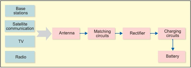
RF sources
Radio waves, which are part of the electromagnetic spectrum, consist of magnetic and electrical components. These carry information by varying a combination of amplitude, frequency and phase of the wave within a frequency band. On contact with a conductor such as an antenna, electromagnetic (EM) radiation induces electrical current on the conductor’s surface, which is known as skin effect.
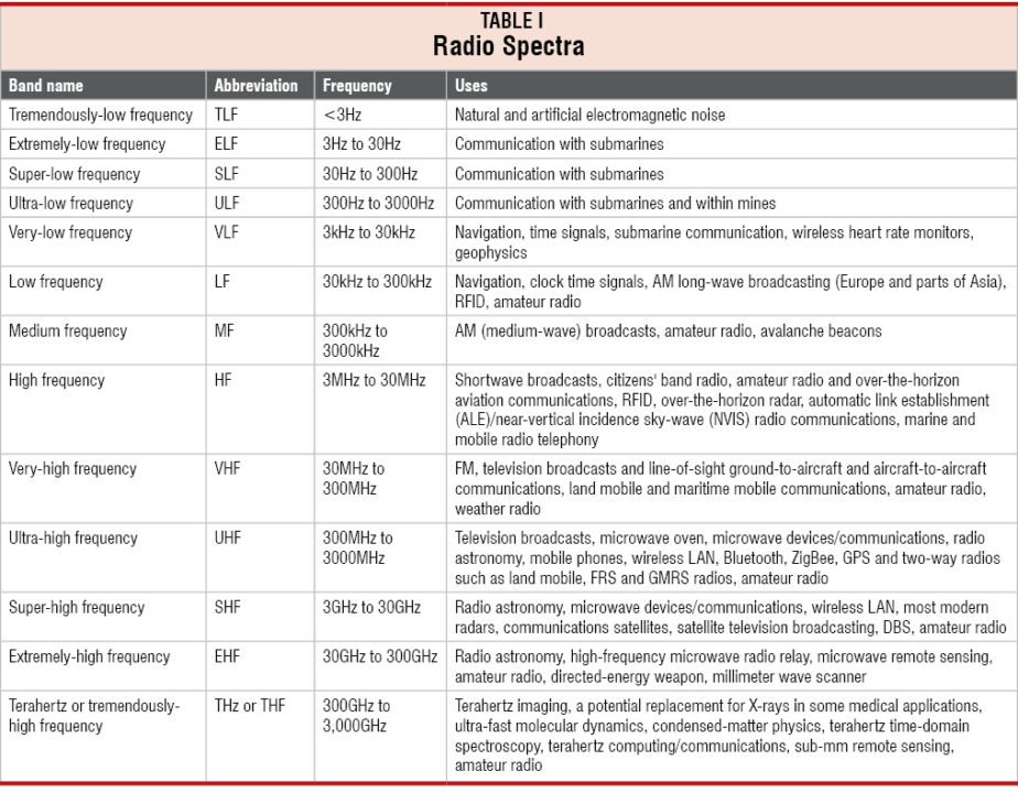
Communication devices use antennae for transmission and/or reception of data by utilising different frequency spectrums ranging from 10kHz to 30kHz. Maximum theoretical power available for RF energy harvesting is 7.0μW and 1.0μW for 2.4GHz and 900MHz frequencies, respectively, for a free space distance of 40m. Path loss of signals will be different in environments other than free space. Table I shows different frequency spectra and its special applications.
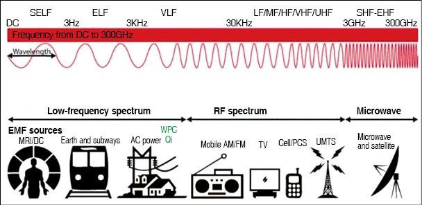
Different frequency bands have different applications. Fig. 1 shows the electromagnetic spectrum with different applications surrounding us.
Components of an RF energy-harvesting system
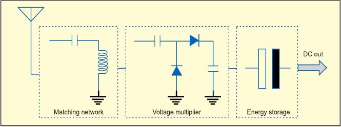
Fig. 3 shows the components of an energy-harvesting circuit. Incident RF power is converted into DC power by the voltage multiplier. The matching network, composed of inductive and capacitive elements, ensures maximum power delivery from the antenna to the voltage multiplier. The energy storage ensures smooth power delivery to the load and as a reserve for durations when external energy is unavailable. Such a design needs to be carefully crafted; increasing the number of multiplier stages gives higher voltage at the load and reduces current through the final load branch. This may result in unacceptable charging delays for the energy-storage capacitor.
Conversely, fewer stages of the multiplier ensures quick charging of the capacitor, but voltage generated across it may be insufficient to drive the sensor mote (at least 1.8V that becomes +Vcc for Mica2 sensors).
Along similar lines, a slight change in the matching circuit parameters significantly alters the frequency range in which the efficiency of energy conversion is maximum, often by several MHz. Hence, RF-harvesting circuits involve a complex interplay of design choices, which must be considered together. This problem is addressed by considering a multi-stage design of the voltage multiplier, whose operating points are decided by solving an optimisation framework.
 Antenna
An antenna is a metallic device (like a rod or wire) for radiating or receiving radio waves. It is a means of transmitting and receiving radio waves. In other words, an antenna is a transition structure between free space and a guided device. The guided device or transmission line may take the form of a coaxial line or a hollow pipe (waveguide), and is used to transport electromagnetic energy from the transmitting source to or from the antenna to the receiver.
Communication devices generally have omni-directional antennae that propagate RF energy in most directions. This maximises connectivity for mobile applications. Energy transmitted from the wireless sources is much higher, up to 30W for 10GHz frequency, but only a small amount can be scavenged in the real environment. The rest is dissipated as heat or absorbed by other materials.
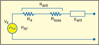
An antenna is required for harvesting RF energy. In an RF energy-harvesting system, the antenna (as receiver) intercepts electromagnetic waves passing by and converts these into electrical signals. A typical antenna can be modelled as AC voltage source series impedance, as shown in Fig. 4.
PRF is power that is received by an antenna; RS is radiation resistance, which stands for the power used for receiving electromagnetic waves; Rloss is loss resistance, representing the actual resistance including the materials of the antenna and dielectric loss and Xant can either be inductive or capacitive depending on the specific antenna.
There are a number of parameters that antennae designers have to pay attention to. Power gain is the ratio of the maximum power density that an antenna can radiate from a certain angle at an arbitrary distance to power density at the same distance of a hypothetical isotropic antenna. It can be thought of as actual maximum power density over the ideal (loss-less) average power density. The effective antenna aperture is closely related to the available power an antenna can deliver. Some other key parameters include path loss, polarisation, efficiency, directivity and so on.
Rectenna
The device used to harvest RF energy is called a rectenna. It refers to a rectifying antenna. A rectenna converts RF energy into DC energy. A typical rectenna has an antenna, a matching circuit and a rectifier.
A rectenna is a hybrid of an antenna and Schottky diode placed at an antenna’s feed point. It directly converts RF to DC signal. Different topologies are available to work as components of the rectenna. Different topologies have been developed for RF-DC rectifier design, such as charge-pump, differential drive bridge rectifier and gate cross-connected differential-drive bridge rectifier.
Charge-pump rectifier
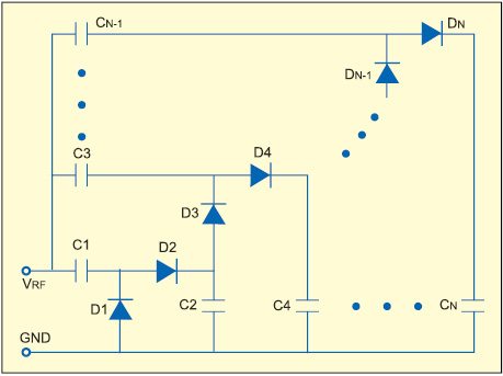
A charge-pump rectifier, also known as voltage multiplier circuit, as shown in Fig. 4, has been widely used in micro power-harvesting circuits. The basic structure of the conventionally-used charge-pump rectifier was proposed in 1976 and originally used as a DC-DC up-converter.

In the RF-DC rectifier application, the circuit is adapted by using RF input as one of the complementary clock signals, and grounding the other clock line and DC input line. To understand the operating principle of the rectifier, first two stages of the multiplier are considered, which are also usually denoted as voltage-doubler.
The operation can be analysed in two cycles: negative half-cycle, where input RF signal is negative, and positive half-cycle, where input RF signal is positive.
Assume, threshold voltage of the diode is VT and amplitude of input RF signal is VRF. In the first negative half-cycle, D1 is conducted and charges are transferred to the right-end plate of C1. At the end of the first negative half-cycle, C1 is charged to VRF -VT.
When the positive half-cycle starts, D1 is reverse-biased and the right-end plate of C1 is pushed to 2*(VRF-VT). D2 is turned on, and charges are transferred to C2. At the end of the positive half-cycle, C2 is charged to 2*(VRF-VT), for a rectifier with more stage doublers.
Differential-drive bridge rectifier
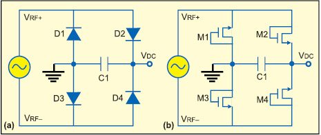
A full-wave bridge rectifier, as shown in Fig. 4, has been commonly used in AC-DC voltage conversion. The rectifier has a differential input RF signal.
In the positive half-cycle of an RF signal, diodes D2 and D3 conduct, while D1 and D4 are reverse-biased.
In the negative half-cycle of the RF signal, diodes D1 and D4 conduct, while D2 and D3 are reverse-biased.
In the whole cycle, load capacitor C1 is charged in a single direction. DC voltage on C1 can achieve VRF-(2*Vth), when the reverse leakage current and other resistive load are considered, where Vth is the threshold voltage of the diodes.
The circuit starts rectifying once amplitude of the input AC signal becomes larger than twice the threshold voltage of the diode, which reduces the voltage sensitivity of the rectifier. To improve voltage sensitivity, a gate-drain-connected n-type metal oxide semiconductor field effect transistor (MOSFET) or gate-source connected p-type MOSFET with low-threshold voltage can be used instead of the diode, as shown in Fig. 6(b). To increase DC voltage level, a stack architecture is applicable by cascading the single-cell bridge rectifier in stages by employing coupling capacitors for DC blocking.
Gate cross connected differential-drive bridge rectifier
Although by using the diode-connected MOSFET with low-threshold voltage, voltage sensitivity of the bridge rectifier can be effectively improved, reverse leakage power consumption induced by the MOSFET is not negligible.
An adapted architecture of the conventional bridge rectifier is to bias the gate terminal with the differential input RF signal. By biasing the gate terminal, turn-on voltage of the MOSFET is reduced, with which voltage sensitivity can be effectively improved.
Consider the architecture in Fig. 7(a) as an example. In the positive half-cycle of the RF signal, as in a normal bridge rectifier, M2 and M3 conduct, while M1 and M4 are reverse-biased. The change happens in the bias voltage in the gate terminal of M1 and M3.
In the positive half-cycle, M3 conducts with a bias signal larger than zero (ground potential) as in a conventional bridge rectifier, which reduces threshold voltage of M3 and hence improves voltage sensitivity.
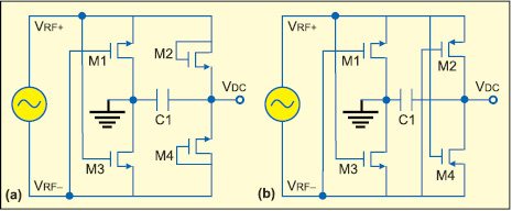
In the positive half-cycle, drain and source terminals of M1 are exchanged. M1 is reverse-biased at the gate terminal with the negative RF signal, which is lower than the ground potential of the source terminal. With such a bias, leakage current induced by M1 is largely reduced.
The same analysis can be done for the negative half-cycle. In an NMOS gate cross-connected bridge rectifier, only two MOSFETs are biased differentially.
To further improve the performance of the rectifier, two PMOS devices are used instead, as shown in Fig. 7(b). In the positive half-cycle, PM2 and NM3 are conducted, while NM1 and PM4 are reverse-biased. Bias signal at the gate terminal of PM2 is negative, which results in a smaller turn-on voltage than the diode-connected mode. Source and drain terminals of PM4 exchange. Gate terminal of PM4 is biased with the positive RF signal, which is larger than the potential at its source terminal and hence reduces the reverse leakage current. The same analysis can be done for the negative half-cycle.
Commonly-used devices for rectifier design are MOSFETs and Schottky diodes. The difference in physical construction results in the disadvantages and advantages in the application of an RF-DC rectifier design. Table II summarises the pros and cons of both devices.
Feel interested? Check out other tech focus articles.


 Antenna
hii,
I wanted to know that, it is possible to do this project pratically. How to deal with multiplier stage.