The method scales up wafer size and improves reproducibility, marking a significant step forward in semiconductor development for AI and cognitive computing.

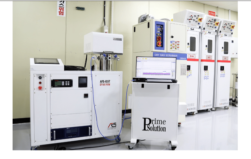
As artificial intelligence (AI) technology advances, there is a rising need for high-performance semiconductors. The development of innovative materials and structures has become essential to meet these demands.A 4-inch heterostructure fabrication technology using plasma-enhanced chemical vapor deposition (PECVD) has been developed, marking the first time globally this method has been applied to semiconductors. This advancement paves the way for low-power, high-performance semiconductors that exceed the capabilities of traditional silicon-based technology.
Led by Senior Researcher Hyeong-U Kim from the Korea Institute of Machinery and Materials (KIMM), in collaboration with Professor Taesung Kim’s team at Sungkyunkwan University, the research team achieved the first 4-inch heterostructure semiconductor using PECVD. This technology, anticipated to enhance AI semiconductor performance, incorporates next-generation materials like transition metal dichalcogenides (TMDc), which offer atomic-level 2D structures with silicon-like performance and low power usage, ideal for machine learning and cognitive computing.

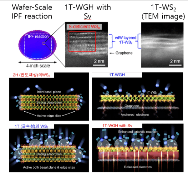
Using PECVD, the team successfully fabricated two types of 4-inch heterostructures. The first combined tungsten disulfide (WS₂) with graphene by depositing a 1-nanometer tungsten layer onto a graphene wafer and treating it with H₂S plasma. Additionally, they created a metal-semiconductor heterostructure using two forms of molybdenum disulfide (MoS₂) as thin films. This process produced a 4-inch wafer with the 1T phase, a challenging achievement due to its metastable nature compared to the stable 2H phase.

Traditional methods for producing heterostructures faced size limitations and reproducibility issues, limiting them to microscale production. The new PECVD technique allows for 4-inch wafer production, supporting larger, reproducible wafers for efficient 3D integrated structures that reduce power loss and heat, making it ideal for AI semiconductor applications. The team emphasized that this technology not only meets scalability and reproducibility requirements but also enables experimental validation previously limited to academia. PECVD is already widely used in the semiconductor industry, so this innovation holds significant potential for commercial mass production.


