Numerous analogue components and chips are introduced to the market every year, but what is influencing their evolution? Read on to find out the latest technologies in this field, the influence of the Internet of Things (IoT) paradigm on analogue world and some interesting applications powered by analogue components.
By Anagha P
Thirty years ago, almost all the technology surrounding us was analogue. However, in the past decade we have witnessed a massive shift from analogue to digital electronics. The digital platform offers amazing opportunities for innovation, and is thus promptly taking over several aspects of modern life.
Will the digital world be able to completely take over analogue technologies and devices? Don’t think so. What we found is that analogue is still well-established, and innovative technologies and products are continuing to emerge in this sector. What is driving this ‘old’ technology?
Influence of IoT
The IoT is perhaps one of the most discussed technology topics these days. It provides a huge opportunity for us to leverage the Internet infrastructure to put technology to better use. Its biggest enabler is the ability to connect the real world with the digital world, thus enabling people and machines to know the status of hundreds of thousands of objects simultaneously.
Analogue components are the key to deliver this connection between the real and digital worlds.
While back-end of the IoT is communication and connectivity forming the digital side, the front-end generally consists of sensors (temperature, pressure, motion, tilt, acceleration, shock, proximity, gas, sound, pH, infrared, etc), actuators, power management modules (linear regulator, converter, battery charger), signal acquisition modules, amplifiers, signal processors, microcontrollers and integrated chips; this is where analogue comes into play.
New component design elements
Form factor and power are major considerations for smart products, and the industry is getting geared up for making analogue devices suitable for IoT segment. However, there are some cases where the size and/or power are not of high relevance, like for the smart-grid applications. Some of the trends driving the analogue industry are discussed in detail below.
Wearable medical devices and low-power components. Many devices, particularly portable and wearable electronics, cannot afford battery-hungry processors and components—even those previously considered as low-power.
This has led to the development of low and ultra-low power devices that can operate for days and months on a single battery, or without the need for recharging. For example, OPA2652 operational amplifiers (op-amps) by Texas Instruments (TI) work at an input current as low as 300nA. On a coin cell it operates for several months together.
Consider a patient-monitoring system. If the instrument is easily drained of all power and has to be charged every few hours, proper monitoring cannot be attained. Moreover, the whole charging process is troubling for the user too.
Benefits of digital in analogue world. The major trick to reduce power is to use low voltage. We want a technology that can be used in analogue devices, operates in low voltages, and also integrates to high voltages. This is where digital was merged with analogue.
For example, filtering is typically done in analogue domain using active filters. But the problem is that, these filters are not tuneable individually and they consume high power. By transferring the signal to the digital domain and performing the filtering there, the filters become individually tuneable and can be switched off when not in use, which reduces power.
Harvesting ambient light. The integrated boost regulator ADP5090 by Analog Devices Inc. is one example where firms have come up with devices that can store energy from indoor ambient light and use the devices to power the sensors.
The ambient light is something that is freely and abundantly available in India throughout the year. Exploiting this natural resource as a viable power source has become a growing trend in wireless sensor network applications worldwide. It eliminates the need of power sources like batteries. In addition, it opens up huge possibilities of enabling IoT and connecting even remote/rural areas to the grid without the need for connected power or batteries.
Size and weight. No surprise that, just like lower power, size and weight of the gadget can also be an important consideration in the portable and wearable electronic space. There is a huge demand in market for smaller and lighter instruments. Size reduction is being achieved by merging circuit topology (whether the same block can be reused in multiple places) and different process technologies.
Integrating different sensors for higher scalability. Sometimes the same application may require low-speed and high-speed sensing. Depending on the condition the application may switch back and forth between low-speed sensing and high-speed sensing.
The typical approach would be using two separate ADCs, one for low speed and the other for high speed, and keep one powered off when the other is being used.
However, when you use a device with wider range you can save space and money, the designing is easier, failure rate is reduced with fewer devices, and the power required is almost the same. Highly scalable devices also become useful in low-power applications. In IoT the power has to be locally derived through photocell or thermoelectric voltage generator.
The supply voltages generated by these are subjected to large variations. One need not worry about regulation in it, if they have an op-amp that can work over such large range; it avoids any intermediate stage of regulation.
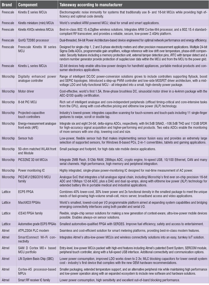
Expandable platforms. It is very important to be able to incorporate new hardware and software solutions to a system in order to produce a better end product. As a result, it is very critical to have a flexible and expandable design platform that is compatible to and can incorporate both new hardware and software solutions, whenever necessary. Microchip’s PIC16(L)F170X and PIC16(L)F171X family of 8-bit microcontrollers offers intelligent analogue and core-independent peripherals (configurable logic cell, complementary output generator and zero crossing detector), providing increased flexibility for designers.
Somsubhro Pal Choudhury of Analog Devices believes that, the wide range of different types and sizes of data, bandwidth availability, reliability and cost considerations will not make a ‘one size fits all’ model. “Customisations and optimisations for each market vertical and sub-vertical would be the key with the industry severely fragmented, at least in this decade,” he adds.
Dedicated processors. There has been a lot of talk about dedicated microcontrollers. Many original equipment manufacturers and fabrication plants are working on process technologies that could create processors optimised for and committed specifically to the analogue implementation in IoT applications.
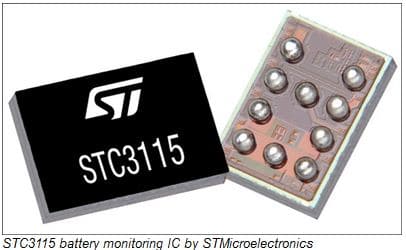
In-built battery monitoring. As wearable devices are run by small batteries, it is necessary to optimise the use of these power sources. An accurate battery monitoring allows the user to know the exact state of charge of battery and adds intelligence to its usage.
For example, STC3115 battery monitoring IC by STMicroelectronics could give timely alert to the user for turning off the power-consuming blocks when battery is lower than the user-programmed threshold levels.
Innovative technologies driving cutting-edge analogue components
Shrinking the size and increasing performance has always been the challenge in semiconductor industry. The semiconductor industry has been witnessing the lowering of cost and size in the last couple of decades. Process nodes have been going from 45nm down to 28nm to 20nm, and will further go down to 16nm and 10nm in the next decade.
But the manufacturers’ challenge was to achieve spatial, monetary or power efficiencies. Hence, as the limit of Moore’s law reached 28 nm, they had to migrate from planar CMOS to a new process technology. That is when devices using FinFET technology were demonstrated by Taiwan Semiconductor Manufacturing Company.
Multiple fin-height FinFETs. The most advanced semiconductor technology used today can produce around 10 million transistor elements in a chip of size one square centimetre. A new multiple fin-height FinFET process technology has been developed at National Nano Device Laboratories (NDL), National Applied Research Laboratories (NARLabs). It allows up to 20 million transistors in the same place, which is twice the number possible today!
Unlike the traditional field-effect transistors (FETs), where gate controls source-drain current only on one side, the fin field-effect transistor (FinFET) has three-dimensional fork-shaped gate similar to a fish’s fin (hence the name). It can control the source-drain current in the transistor from three sides—left, right and top. In multiple fin-height FinFET, like the name suggests, the fins will have different heights allowing different amount of currents corresponding to associated channel height. This concept lets further reduction in chip area by 20%. Compared to a normal FinFET, the multiple-height FinFET has 20% higher storage capacity and 20% less manufacturing cost.
FD-SOI. STMicroelectronics, along with its partners, introduced a technology known as Fully Depleted Silicon On Insulator (FD-SOI). It is a planar process technology where an ultra-thin layer of insulator (buried oxide or BOX) is positioned on top of the base silicon and then a very thin silicon film implements the transistor channel.
IC etched on graphene. Several manufacturing units have been working on moving from silicon to other alternatives, to get better performance in terms of power, size and cost. These alternates could be based on graphene, nanotubes or various tunnel field-effect transistors (TFETs).
There is on-going research on these and other devices based on electron spin as opposed to electron charge. Researchers at University of California, Santa Barbara, have come up with the concept and demonstration of an integrated circuit design scheme where the transistors and interconnects are monolithically patterned seamlessly (without obvious joints or seams) on a two-dimensional atomically flat sheet of graphene.
The model of etching offers possibilities for extremely energy-efficient, transparent and flexible next-generation green electronics.
Photonic IC that can manipulate atoms. A group of scientists from California State University, Pasadena, claim to have developed an optical circuit that uses light to manipulate individual atoms in small, self-contained units. According to them, the photonic integrated circuit is an integrated optical circuit with a photonic crystal that can both localise and interface atoms with guided photons in the device.
The optical properties of photonic crystals are determined by factors like their physical geometry and size of the waveguide. This feature allowed the scientists to make a photonic crystal of silicon nitride that acts as waveguide for laser light tuned to certain atomic transitions in caesium. The caesium atom absorbs and scatters these wavelengths, generating forces that could trap and manipulate the atom.
The photonic crystal is integrated into a small, self-contained system that has a readily available supply of caesium atoms. These units are relatively cheap to make and easy to operate. This interesting technology could serve as high-quality building block for quantum computation and communication. It also opens door for several experimental opportunities.
Analogue standing tall
Over the last few years, we have witnessed the shifting of electronics world from analogue to more sophisticated and efficient digital substitutes. But all analogue components cannot be completely substituted by digital devices; they would coexist and complement each other. With the extensive developments in the IoT segment, we see it driving many new technologies and products in analogue components and chips.
The author is a dancer, karaoke aficionado, and a technical correspondent at EFY.


