An electronic stacking method could significantly increase the number of chip transistors, improving AI hardware efficiency.

MIT engineers have created a new type of chip that doesn’t need silicon wafers and works at lower temperatures to protect the circuits underneath. This method lets them build chips with materials stacked directly on each other, allowing components like transistors and memory to be placed on any crystal surface. This design improves communication between layers, and the researchers think it could lead to AI hardware, such as stacked chips for laptops or wearables, that are as fast and capable as today’s supercomputers.
The team aimed to refine their method to grow single-crystalline 2D materials at lower temperatures that wouldn’t damage the underlying circuitry. They discovered a solution in metallurgy — the science of metal production. When molten metal is poured into a mould, it slowly forms grains that grow and merge into a regular crystal pattern as it cools and hardens. Metallurgists have found that this nucleation process happens most efficiently at the edges of the mould where the liquid metal is poured.
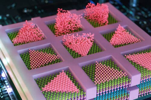
The team aimed to grow single-crystalline TMDs on a silicon wafer already containing transistor circuitry. As in their earlier work, they covered the circuitry with a silicon dioxide mask and then deposited TMD “seeds” at the edges of the mask’s pockets. These edge seeds grew into single-crystalline material at temperatures as low as 380 degrees Celsius. In contrast, seeds placed in the centre of the pockets required higher temperatures to form single crystals.
Building on this, the researchers used the method to create a multilayer chip with alternating layers of two different TMDs — molybdenum disulfide for n-type transistors and tungsten diselenide for p-type transistors. These materials, crucial for logic operations, were grown in single-crystalline form directly on each other without needing intermediate silicon wafers. Kim states that this method could effectively double the density of semiconducting elements on a chip, especially for metal-oxide semiconductors (CMOS), a key component in modern logic circuits.


