


This innovation aims to accelerate the discovery of new solar cell materials and integrate into a fully automated materials screening system, promising significant advancements in solar energy, transparent electronics, and transistors.
Boosting the performance of solar cells, transistors, LEDs, and batteries requires electronic materials, which are yet to be discovered. To expedite this process, scientists are employing AI tools to identify promising materials from a vast pool of chemical formulations. Concurrently, engineers are developing machines capable of printing hundreds of material samples based on AI-tagged chemical compositions.
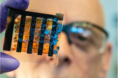
Despite advances in AI and automated printing, the characterization of printed materials remains a significant bottleneck. Traditionally, this step involves slow, manual analysis to confirm that the materials perform as expected. MIT engineers have now introduced a computer vision technique that dramatically speeds up the characterization of newly synthesized electronic materials. This method automatically analyzes images of printed semiconductor samples and swiftly estimates two critical properties: band gap (electron activation energy) and stability (longevity). The new technique is 85 times faster than the current standard approaches. The researchers aim to use this technique to accelerate the discovery of new solar cell materials. They envision integrating this method into a fully automated materials screening system.

Harnessing the Power of Optics
Typically, a “domain expert” manually characterizes each new material using a benchtop tool called a UV-Vis. This tool scans different colors of light to determine where the semiconductor begins to absorb more strongly. While precise, this method is slow, handling about 20 samples per hour compared to machines that can print 10,000 combinations per hour. To address this disparity, Buonassisi and colleagues turned to computer vision, which uses algorithms to analyze optical features in images quickly and automatically. The team developed two computer vision algorithms. The first processes hyperspectral images with 300 channels, transforming the data to compute the band gap swiftly. The second algorithm analyzes standard RGB images to assess a material’s stability by observing color changes over time.
The team mentioned that they have found that color change can be a good proxy for degradation rate in the material system we are studying, Ultimately, they envision fitting this technique into an autonomous lab of the future. The system would allow them to give a computer a materials problem, have it predict potential compounds, and then run 24-7 making and characterising those predicted materials until it arrives at the desired solution.The application space for these techniques ranges from improving solar energy to transparent electronics and transistors.
