Utilizing an approach to synthesize single-crystalline metal nanosheets for 2D substrates, this process addresses compatibility issues with atomic-layer deposition (ALD) techniques and opens new possibilities for high-performance electronics.
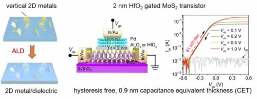
Researchers at Nankai University in China have unveiled a method to integrate extremely thin insulating layers with two-dimensional (2D) semiconductors, paving the way for the creation of 2D transistors with electrical capacitance akin to SiO2, even below 1-nm thickness. This promises to enhance the performance and energy efficiency of electronic devices. The team introduced a novel strategy to synthesize single-crystalline metal nanosheets that can be transferred onto 2D substrates. Published in Nature Electronics, their approach successfully deposited 2-nm-thick dielectrics made of Al2O3 or HfO2, facilitating the development of high-performance top-gated transistors.
Reviewing existing literature, the researchers noted that Pd and Au-based 2D metals had not yet been synthesized using CVD. They observed that 2D metal nanosheets have atomically flat surfaces and can be vertically grown on substrates. This led to the idea of integrating these vertically grown 2D metals with atomically thin, atomic-layer-deposited (ALD) dielectrics to avoid compatibility issues between ALD and 2D semiconductors. The team deposited atomically thin dielectrics, specifically Al2O3 and HfO2, on vertically grown 2D metals. Unlike molybdenum disulfide (MoS2), commonly used as a semiconductor in transistors, 2D metals are compatible with ALD techniques. After ALD growth, the metal/oxide stack can be integrated with 2D semiconductors in a single step, forming a van der Waals interface.

This approach facilitates the fabrication of 2D transistors with sub-nanometer capacitance equivalent thickness. The researchers used their CVD strategy to create 2-nm-thick dielectrics and fabricated top-gated transistors, which demonstrated promising results, including leakage currents of 10−6 A cm−2, low operating voltages of around 0.45 V, and hysteresis below 1 mV. They highlighted that their Bi2O3-assisted CVD growth method marks a significant advancement in the synthesis of new 2D materials. The team aims to achieve wafer-scale fabrication of hysteresis-free 2D transistors with capacitance equivalent thickness below 1 nm.
“Our initial goal was to develop a chemical vapor deposition (CVD) strategy for 2D Cu2O, a high-mobility p-type semiconductor,” explained Jinxiong Wu, the study’s corresponding author, to Tech Xplore. “However, using CuCl and Bi2O3 as precursors, we ended up with elemental Cu metal. By altering the metal chlorides, we could also produce 2D metals like Pd and Au.”