The resulting MoS2 FETs showed mobilities of 21 cm²/Vs, contact resistances of 3.8 kΩµm, and on-current densities of 120 µAµm⁻¹, similar to single-crystalline fakes.

Electronics engineers have been designing more sophisticated transistors that can be scaled to smaller sizes. Conventional silicon-based field effect transistors (FETs) have limitations, prompting some teams to explore materials with higher electron mobility. Transition metal dichalcogenides (TMDs) are promising materials for scalable FETs due to their small size and good carrier mobility. Molybdenum disulfide (MoS2), a compound with molybdenum and sulfide atoms, is one such material.
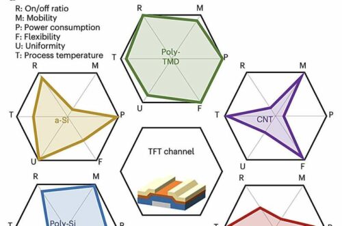
Researchers at Samsung Advanced Institute of Technology (SAIT) and Seoul National University recently integrated MoS2 transistors on a 200 mm wafer. Their work demonstrates the scalability of MoS2-based transistors, highlighting their potential for smaller and flexible devices. They noted that two-dimensional semiconductors are suitable for thin-film transistors due to their scalability, transferability, atomic thickness, and relatively high carrier mobility. The researchers addressed a performance gap between single-device demonstrations, which typically use single-crystalline two-dimensional films, and devices integrated on a large scale using industrial methods. They reported the 200-mm-wafer-scale integration of polycrystalline MoS2 FETs.
Enhanced PerformanceUsing MOCVD
The team fabricated large-scale arrays of MoS2 FETs using metal-organic chemical vapor deposition (MOCVD). They eliminated the Schottky barrier at the interface between the MoS2 material and metal, enhancing the FETs’ carrier mobility. Their fabrication strategy is compatible with current electronic manufacturing processes. The researchers processed their FETs at a commercial facility, achieving a yield of over 99.9%. The team noted that the metal–semiconductor junction in polycrystalline MoS2 differs from its single-crystalline counterpart, leading to a redesign of the process flow to nearly eliminate the Schottky barrier height at the metal–MoS2 contact.
Initial tests showed that these FETs outperformed other MoS2-based FETs in field-effect mobility, contact resistance, and on-current densities. The team attributed this performance to new fabrication steps that eliminated the Schottky barrier and reduced contact resistance.The researchers identified factors contributing to performance differences, including the lack of impurities on the contact and preventing MoS2 materials from peeling off. When integrated on a 200 mm wafer, the FETs were uniform with slight die-to-die variations.
By employing metal-organic chemical vapor deposition (MOCVD) and addressing the Schottky barrier at the MoS2-metal interface, the team enhanced the carrier mobility and achieved a yield of over 99.9%. Their work demonstrates the scalability and potential of MoS2-based transistors for developing smaller, flexible devices. The successful integration and performance of these FETs highlight the promise of two-dimensional semiconductors for future electronic applications, paving the way for further experimentation and potential large-scale commercialization.


