Stanford researchers have created a new method to improve MoS2 transistors by adding strain using silicon nitride layers, making them better for 2D semiconductor devices.

The manipulation of mechanical strain in materials, or strain engineering, has been a critical factor in advancing electronics over the past few decades, particularly in enhancing device charge carrier mobility. Several recent studies have focused on developing effective methods to control strain in two-dimensional (2D) semiconductors, emphasising compatibility with current industrial processes.
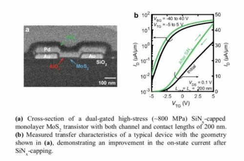
Researchers at Stanford University have recently presented a CMOS-compatible technique for engineering tensile strain (stretchiness) in monolayer semiconductor transistors. This method utilises silicon nitride capping layers to apply strain to monolayer molybdenum disulfide (MoS2) transistors integrated on silicon substrates.
The team’s primary goal in recent work was to identify promising new strain engineering techniques based on the processing of conventional silicon transistors that could be applied to 2D materials. After developing one of these techniques, they successfully applied it to a 2D MoS2-based transistor for the first time.
First, the researchers processed 2D semiconductors using established fabrication techniques to create transistors. At the end of the process, they applied silicon nitride films, which enabled them to precisely isolate the impact of these films on the strain in the transistors, separating them from effects related to temperature fluctuations and doping.
In initial tests, the researchers found that their strain engineering approach improved the performance of 2D MoS2 transistors while reducing both the transistor channels and contacts. This work could pave the way for future development of smaller, higher-performing 2D semiconductor-based transistors.
At a fundamental level, the researchers are using flexible substrates to study the effects of strain on other less well-understood 2D semiconductors. They also investigate different sources of process-induced strain, such as the impact of metal deposition on 2D materials, which is a critical step during device fabrication. The team is also working on extending their approach to p-type 2D transistors, as these devices currently exhibit lower performance than the n-type devices used in this study.


