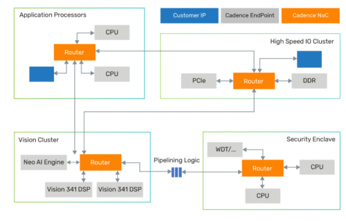
The Cadence Janus NoC allows design teams to achieve improved power, performance, and area (PPA) more quickly and with reduced risk, thereby freeing up valuable engineering resources to focus on SoC differentiation.

Cadence Design Systems, Inc. has expanded its system IP portfolio with the addition of the Cadence Janus Network-on-Chip (NoC). As larger and more complex SoCs and multi-chip systems are developed to meet increasing computational demands, data delivery within and between silicon components has become more challenging, affecting power, performance, and area (PPA). It manages these high-speed communications efficiently with minimal latency, helping customers achieve their PPA targets more quickly and with lower risk.
Current features and benefits include:
- Easy configuration: GUI enables easy NoC configuration from small subsystems to full SoCs and future multi-chip systems.
- Accelerated time to market: PPA-optimized RTL helps SoC designers meet bandwidth and latency goals. Packetized messages enable higher utilization of wires, reducing wire count and timing closure challenges.
- Lower risk: The NoC’s built-in power management, clock domain crossing, and width matching reduce design complexity.
- Quick turnaround: Simulation and emulation capabilities enable early architectural exploration, allowing quick validation of PPA results to ensure the configuration meets design requirements.
- Scalable architecture: Customers can design a subsystem and reuse it in a full SoC context, allowing future reuse in a multi-chip system.
- Flexibility: The NoC is compatible with any IP with an industry-standard interface, including AXI4 and AHB.
The NoC utilizes the company’s Tensilica RTL generation tools. Customers can use its software and hardware for simulation and emulation of their NoC and gain insights into its performance using System Performance Analysis tool (SPA). This flow enables architectural exploration, resulting in the best NoC design for product needs. The NoC addresses routing congestion and timing issues associated with complex SoC interconnects, which often become apparent only during physical implementation. It also supports industry-standard memory and I/O coherence protocols.
“We support Cadence’s investment in system-level solutions,” said Suk Lee, VP and GM, Ecosystem Technology Office at Intel Foundry. “As a NoC is essential for almost any subsystem in today’s SoCs, we look forward to Cadence continuing to expand their IP offering.” “Cadence is a recognized leader in IP and design quality, and we continue to invest in our interface and processor IP, system IP, software, and design services capabilities to enable our customers to develop differentiated designs,” said Boyd Phelps, senior vice president and general manager of the Silicon Solutions Group at Cadence. “The addition of the Cadence Janus NoC to our system IP portfolio is a significant step in this strategy. Transitioning from an IP provider to an SoC design partner allows us to deliver greater value to our customers, enabling them to focus on differentiating their silicon.”


