New platform offers industry’s highest resolution at 8.3MP combined with most advanced automotive system level features
Consumer Electronics Show (CES) – Venetian 3302 – LAS VEGAS, NV – 5 January, 2018 – ON Semiconductor, driving energy efficient innovations, today announced a scalable family of CMOS image sensors to address the spectrum of applications for Advanced Driver Assistance Systems (ADAS) and autonomous driving. ON Semiconductor’s newest sensor family offers car makers and tier one suppliers a choice of robust imaging devices based on a common platform and feature set. The sensors have resolutions scaling from 8.3 megapixels (MP) down to 1.2 MP with industry leading low-light performance from 4.2 µm pixels. Additional features include functional safety up to ASIL-C, high-dynamic range (HDR), an industry-first cybersecurity option, and second-generation wafer stacking technology that reduces package size. Individual products in this platform are currently under evaluation by many technology partners, including Mobileye and NVIDIA for use with its DRIVE AI computing platform for autonomous vehicles.
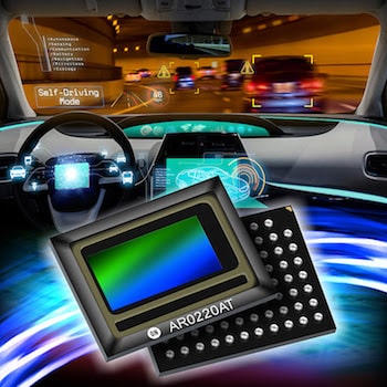
The AR0820AT, AR0220AT and AR0138AT form a scalable image sensor family which provides a range of resolutions suited to new-generation ADAS and autonomous driving systems. Automakers need different resolutions to address segmentation in their product lines, where specific safety features are standard, but additional cameras or higher resolution cameras enable more advanced safety and luxury capabilities as customer options.
As the industry moves from Level 2 systems for emergency autonomous braking, adaptive cruise control and lane change assistance towards fully autonomous driving, ON Semiconductor’s image sensors enable increasingly demanding ADAS and autonomous driving capabilities. The large 4.2 µm pixel delivers leadership performance in low-light scenarios such as night-time emergency braking for pedestrians and cyclists that is being added to safety tests defined by Euro NCAP. The family’s cybersecurity technology helps ensure reliable and secure operation when multiple cameras around the vehicle are connected to a centralized system where data and commands must travel by wires between the sensor and the processor.
For advanced imaging capabilities, software and algorithm testing is typically the longest task in the development program. With ON Semiconductor’s family of scalable image sensors, customers can start early development with one sensor to adapt their algorithms to the pixel performance and system features, and then extend to additional resolutions with further testing. This shortens project time-to-market and reduces overall development costs across a family of camera system implementations.

“As the number of image sensors on a vehicle increases, having a scalable platform with common core features and pixel architecture becomes even more important for automakers to deliver new safety and self-driving features to market quickly and efficiently,” said Ross Jatou, vice president and general manager of the Automotive Solution Division at ON Semiconductor. “Our deep engagement with customers and the advanced features of our new image sensor family enable them to bridge development efforts across ADAS and autonomous driving programs.”
ON Semiconductor will be demonstrating its new family of scalable image sensors, plus a wide range of other leading edge semiconductor-based solutions for automotive and other sectors at The Sands Convention Center/Venetian (Murano 3302) during CES 2018, January 9-12 in Las Vegas. The company’s imaging experts will be available all week to answer questions regarding solutions for automotive image sensor applications.


