


This paves the way for advancements in wearable sensors, customizable robots, and medical devices, promising to transform manufacturing processes and reduce prototyping complexities.
Researchers at the University of Missouri have pioneered a method to fabricate complex devices using multiple materials, including plastics, metals, and semiconductors, with a single machine. This research introduces the Freeform Multi-material Assembly Process, which leverages a novel 3D printing and laser technique to create multi-material, multi-layered sensors, circuit boards, and even textiles embedded with electronic components.
The new process enables the integration of sensors within structures, allowing the creation of objects capable of sensing environmental conditions like temperature and pressure. This advancement holds significant potential for various applications, such as natural-looking sensors for oceanic research and wearable devices for monitoring vital signs. This is the first time this type of process has been used, and it’s unlocking new possibilities, researchers claimed. One key advantage of this technique is that it allows innovators to focus on designing new products without the complexities of prototyping. They highlighted the broad impact this could have on industries like wearable sensors, customizable robots, and medical devices. It will broadly impact wearable sensors, customisable robots, medical devices, and more.

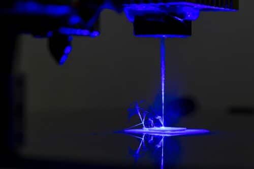
Traditional manufacturing of multi-layered structures, such as printed circuit boards, is often cumbersome, costly, and environmentally unfriendly. The new method, inspired by natural systems, addresses these challenges by using a three-nozzle machine: one nozzle applies ink-like material, another uses a laser to shape materials, and the third adds functional materials to enhance product capabilities. This process begins with standard 3D printing filament and then employs a laser to convert parts into laser-induced graphene, followed by the addition of further materials to enhance functionality. The team emphasized the commercial potential of this technology, particularly through the I-Corps program, which is helping to identify market needs. They believe it will ultimately benefit businesses by shortening fabrication time for device prototyping.
