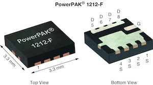
The 30 V n-channel power MOSFET features source flip technology, providing power density and thermal performance for various applications.

Vishay Intertechnology, Inc. has introduced a new 30 V n-channel TrenchFET Gen V power MOSFET, the Siliconix SiSD5300DN, designed for industrial, computer, consumer, and telecom applications. This device features source flip technology in the 3.3 mm by 3.3 mm PowerPAK 1212-F package, offering on-resistance of 0.71 mΩ at 10 V and a figure of merit (FOM) for switching applications of 42 mΩ*nC.
Due to its source flip technology, the device provides lower on-resistance, increases power density, and reduces thermal resistance from 63 °C/W to 56 °C/W. The device’s FOM is better than previous-generation MOSFETs, leading to lower conduction and switching losses, which is beneficial for energy saving in power conversion applications.
The package source flip technology alters the proportions of the ground and source pads, enlarging the ground pad area for more efficient thermal dissipation and cooler operation. It also minimises the switching area to mitigate trace noise. Specifically, the package’s source pad size is increased from 0.36 mm² to 4.13 mm², improving thermal performance. Additionally, the package’s centre gate design facilitates the parallelization of multiple devices on a single-layer PCB.
Some of the key specifications of the PowerPAK 1212-F package include:
- Package size: 3.3 mm x 3.3 mm
- Source pad dimension: 4.13 mm²
- Thermal resistance: 56 °C/W
- Lowest available on-resistance in Gen V technology: SiSD5300DN: 0.87 mΩ (maximum)
The MOSFET is suited for applications such as secondary rectification, active clamp battery management systems (BMS), buck and BLDC converters, OR-ing FETs, motor drives, and load switches. It can be used in various end products, including welding equipment, power tools, servers, edge devices, supercomputers, tablets, lawnmowers, cleaning robots, and radio base stations.


