

Designed for comprehensive SEMI Inspection, including Advanced WLP/PLP and SEMI Back-End Package processes, the platform supports ultra-high-speed TSV inspections.
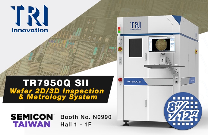
Test Research, Inc. (TRI) announced the latest in AI-powered Automated Optical Inspection (AOI) solutions tailored for the Semiconductor and Advanced Packaging Industry. TRI’s comprehensive SEMI Inspection solutions cater to Advanced WLP/PLP and SEMI Back-End Package processes. It unveil the new TR7950Q SII Wafer Inspection Platform. This advanced system features a 25MP camera with 2.5 μm resolution and a 12MP camera with a 0.55 μm microlens, enabling high-resolution 2D/3D DFF inspection. Equipped with AI-powered inspection algorithms, the TR7950Q SII is designed for Wafer Macroscopic 3D Inspection and micro measurement metrology.
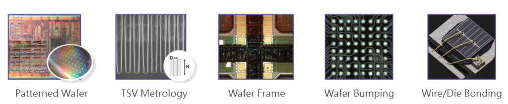
It supports the inspection of Advanced WLP, Wafer Frame, Patterned Wafer, Wafer Bumping, WLCSP, through-silicon via (TSV), and more. The TSV module, provided by OmniMeasure, allows the TR7950Q SII to perform ultra-high-speed TSV inspections, including sensing TSV depth, trench depth, and film thickness for oxide, nitride, PR, and PI films. The key features include:

• 3.5 μm High-Resolution 3D SEMI Back-end, Mini-LED and 008004 solder inspection
• Advanced Wide Spectrum Light for Enhanced Contrast and Detection Rate
• Improved Accuracy and Stability for Precise Solder Measurements
• High Precision Inspection for Multiple Applications
• Industry 4.0 Ready Platform
• Ensures clean operation with HEPA Filter*
The company also introduced its latest back-end inspection solutions, including the TR7007Q SII-S and TR7700Q SII-S. The TR7007Q SII-S is designed for inspecting Mini-LEDs, C4 bumps (~100 μm Ø), and 008004 paste applications. Meanwhile, the AI-powered 3D SEMI AOI, TR7700Q SII-S, is capable of inspecting die, wire diameters up to 15 μm (0.6 mil), SiP, underfill, bumps, and more. An X-ray Inspection Demo Station will be featured, showcasing the company’s SEMI AXI solutions for inspecting C4 bumps and Cu pillars. The cutting-edge TGV metrology tool employs non-contact tomography measurement to easily view cross-sections of glass vias and measure side wall angles without the need for SEM.