The LSIs will minimise external interferences, assist reliable communication and consume less power – without any space constraints

Location information using IoT and wearable devices have resulted in increased demand for GNSS receiver LSIs. To ensure proper operation of IoT and wearable devices in environments with unstable and difficult communication networks, precise positioning and reliable communications must be maintained.
Situations such as multipath propagation caused by surface reflection results in a signal disturbance on the receiving end. Additionally, device size constraints require for a compact battery, whereas satellite signal reception and positioning when using GNSS functionality typically consumes a lot of power, resulting in poor battery life.
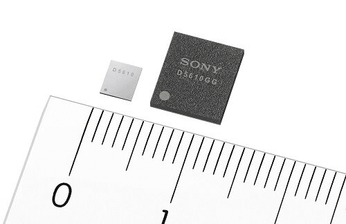
Therefore, Sony Corporation has announced that it will soon be releasing a high-precision Global Navigation Satellite System (GNSS) receiver LSIs CXD5610GF and CXD5610GG for IoT and wearable device applications and will be having low power consumption for dual-band positioning operation.
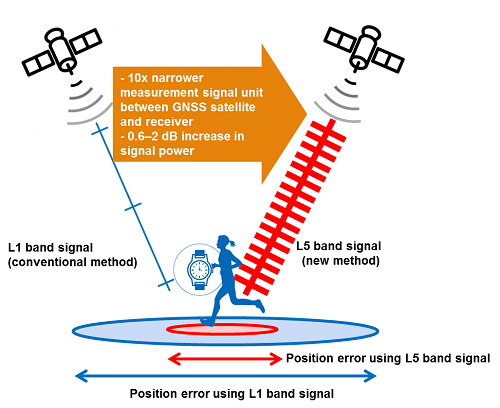
The new LSIs support not only conventional L1 band reception but also the current L5 band reception that is being implemented across GNSS constellations, thereby making them capable of dual-band positioning. Sony’s algorithms enable stable, high-precision positioning for wearable devices even under difficult conditions. Also, the company’s high-frequency analogue circuit and digital processing technologies deliver the low power consumption during continuous positioning for dual-band reception operation, at only 9 mW.
It is expected that the new LSIs will drive greater opportunities to develop new products and services such as smartwatches and other wearable devices that cannot use external power supplies, as well as IoT devices used for applications such as trackers. They also show promise of usage in a wide variety of applications which require precise positioning and stable communications, such as automotive services.

Key Features
- Quick and accurate GNSS signal reception enables more stable positioning than conventional products in environments with fluctuating reception, such as obstruction from buildings when on the move and due to swinging of the arms.
- This also leads to quick positioning time even from cold starts (i.e positioning without the current time, current location or satellite information). Additionally, digital signal processing technology enables countermeasures against the performance degradation caused by radio interference from aircraft communications as well as spoofing attacks and other issues, thereby improving resistance to interference.
- Low power consumption and high sensitivity delivered by analogue circuit technology, which enables low-voltage operation, as well as digital circuits and software algorithms enable software processing via low clock frequencies. This keeps power consumption from only 9 mW to 11 mW when simultaneously receiving signals in both the L1 and L5 bands.
- The new LSI’s feature built-in non-volatile memory for storing firmware, etc. This design makes it possible to update the firmware without adding externally mounted memory and contributes to a more compact design for IoT and wearable devices by saving space. It also makes it possible to complete data-processing in the products, resulting in low power consumption and improved access speed.
- Built-in non-volatile memory for storing firmware makes firmware update possible without adding externally mounted memory and contributes to a more compact design for IoT and wearable devices by saving space. It also enables to complete data-processing in the products, resulting in low power consumption and improved access speed.
The CXD5610GF and CXD5610GG LSIs will be available in XFBGA-54Pin(3.2×3.7×0.5mm) and LFBGA-72Pin (7.0×8.0×1.4mm) respectively from September 2020.


