
The all-stacking technique offers an efficient, high-quality, and universal approach for preparing 2D electronic devices, paving the way for future industrial-level manufacturing of these devices.
In traditional fabrication processes, metal electrode deposition can damage the delicate lattices of 2D materials, degrading their electrical performance. Achieving reliable electrical contact between 2D materials and metal electrodes is essential for improving these devices’ efficiency.
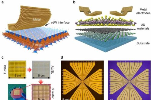
Researchers from the University of Science and Technology of China (USTC) developed an all-stacking technique to achieve reliable 2D vdW contacts. This method allows direct stacking of metal electrodes onto 2D materials, avoiding metal deposition and protecting the materials from damage. This innovative technique optimizes the interface between 2D materials and metal electrodes, promising to revolutionize 2D electronic device performance. Their findings, published in Nature Communications, highlight the potential for enhanced operability and large-scale applications of 2D vdW contacts, which ensure good electrical contact and avoid defects.

Devices fabricated using this technique exhibited sharp metal-semiconductor contact interfaces and smooth, clear vdW gaps with no metal atom doping on the 2D material side. These features indicate the formation of high-quality vdW contact. Transistors made with this technique showed a remarkable 95% reduction in off-state current and a 50% decrease in subthreshold swing compared to those made with traditional metal deposition. They also had a higher on-off ratio, beneficial for low-power integrated circuits.
To showcase the technique’s potential for large-scale manufacturing, the team fabricated an array of field-effect transistors based on monolayer molybdenum disulfide. The device yield was an impressive 98.4%, demonstrating excellent consistency and stability. The average on-off ratio of the transistor array was 6.8×10⁶, with 91.3% of the devices exceeding an on-off ratio of 10⁶. This high performance and consistency highlight the advantages of the all-stacking technique in achieving reliable contact for 2D electronic devices.