

This technique enhances AI processing by drastically reducing power consumption while maintaining high performance, paving the way for the future of next-generation computing.
Artificial intelligence (AI) and machine learning (ML) tools have revolutionised data analysis and prediction tasks but often face challenges due to their high computational and energy demands. Traditional silicon-based processors struggle to meet these requirements, prompting the need for more efficient alternatives. Researchers at Peking University and other Chinese institutions have developed a tensor processing unit (TPU) based on carbon nanotubes (CNTs), offering a promising solution to this challenge. This TPU represents a significant advancement in the quest for next-generation, energy-efficient chips.

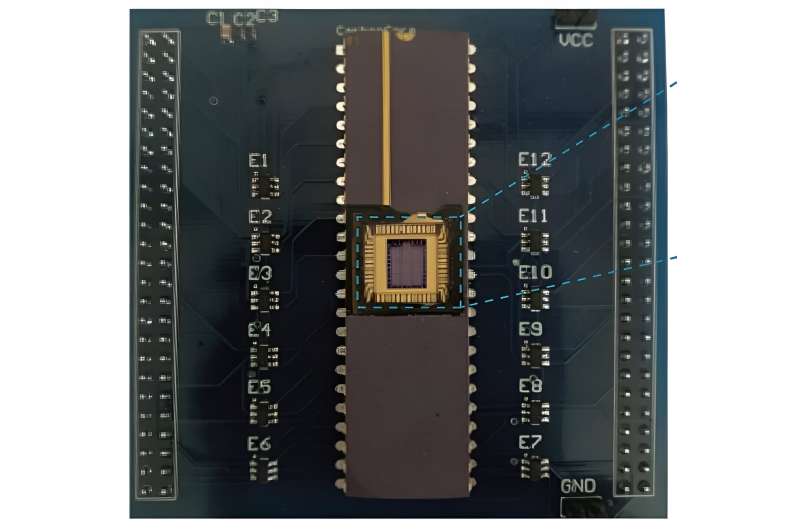
The team mentioned that they have successfully developed the world’s first tensor processor chip (TPU) based on carbon nanotubes. The development was inspired by the rapid growth of AI applications and the limitations of current silicon-based technology in processing massive datasets. They sought to address this global challenge by leveraging the unique properties of carbon nanotubes. The TPU is built on a systolic array architecture, where processors rhythmically compute and transmit data, akin to blood flow in the human body. The researchers employed carbon nanotube field-effect transistors (FETs) to replace traditional semiconductors, creating a more efficient processing unit.
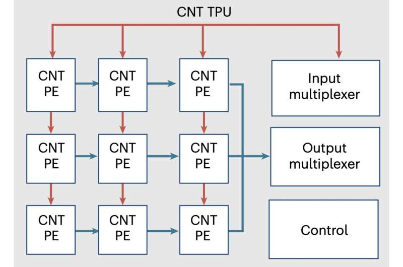
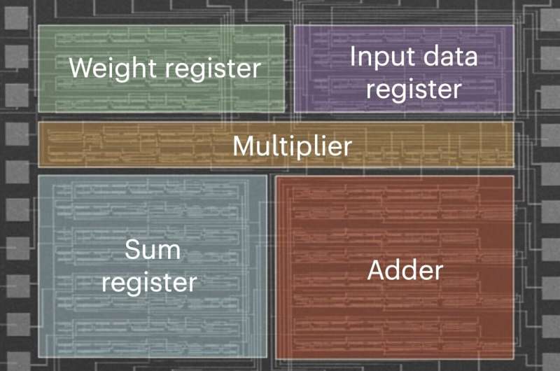
The chip consists of 3,000 CNT FETs arranged in a 3×3 processing unit (PE) matrix, enabling parallel execution of integer convolutions and matrix multiplications. This architecture significantly reduces energy consumption by minimizing static random-access memory (SRAM) operations. Each PE receives data from upstream neighbors, computes partial results, and passes them downstream, efficiently handling 2-bit matrix multiplications.The chip’s design allows for seamless switching between different tensor operations, making it a crucial development in low-dimensional electronics.
The team demonstrated the TPU’s capabilities by building a five-layer convolutional neural network that achieved 88% accuracy in image recognition tasks while consuming only 295μW of power—remarkably low compared to existing technologies. The CNT TPU also showed superior energy efficiency, operating at 850 MHz with energy efficiency exceeding 1 TOPS/w, a notable advantage over current technologies. The success of this CNT-based TPU suggests its potential to enhance AI processing power while drastically reducing energy demands. The research team plans to refine further the chip’s performance, scalability, and energy efficiency, exploring possibilities such as three-dimensional integration with silicon CPUs.