


Transistor is used in almost every electronics appliance or gadget that you see or dream about possessing in near future. Right from that mobile phone which that young college student is so proud of as it makes his life ultra easy to that tiny MCU chip inside a laptop that is helping a motivational speaker to create his YouTube Videos for granting his hard-earned life skills to the general public has one thing in common – the good old transistor.
Transistor is also the main component or we can call it the heart of the Class A amplifier. In this tutorial let’s explore how a Class A amplifier works in an exciting, easy and fun way.
Working of a Transistor
For this, we need to understand the basic working of a transistor, when used in amplifier circuits.
![]()
The above diagram shows the different components that are present inside and outside an NPN transistor. On the top left we have three types of currents I(B), shown in red, I(C), shown in blue and I(E), shown in green. The base terminal is shown as a big red B, while the collector and emitter terminals are shown as big blue C and big green E respectively. There is a big blue gate near the collector terminal which opens up automatically when we open the small pink gate present near the base terminal. So basically a small gate at base can lift up a large gate at collector. The V(CE) is the difference in voltage between Collector and Emitter terminals while V(BE) is the difference in voltage between Base and Emitter terminals. The black arrow on the left of the green Emitter terminal indicates that it’s an NPN transistor type.
![]()
As shown above a small minute current, I(B) at the base terminal causes the small pink gate to open up which in turn causes the large blue gate to open up. As this larger gate opens it allows the large current I(C) to flow from collector to emitter terminal.
![]()
As shown above the base current I(B) and I(C) combine to form emitter current I(E) which ultimately passes to the emitter terminal.
Transistor’s Amplifier Action
![]()
As shown in the above figure a small change in V(BE) causes a change in I(B) which then lifts both pink and blue gates.
![]()
As the pink and blue gates get lifted it directly causes a large change in the collector current I(C). The flow of I(C) causes the difference in voltage between Collector and Emitter terminals to change which ultimately changes the component V(CE).
Thus a small input at base gets amplified as a large output at Collector-Emitter. This amplification action of a transistor is fully utilized in a class A amplifier.
Emitter Junction Works as a Diode
![]()
The Emitter-Base junction of a transistor which is forward biased actually works as a DIODE and offers a small AC resistance to the input signal.
In the figure above (C ), (B) and (E) are Collector, Base and Emitter terminals respectively.
R(C) and R(E) are Collector and Emitter resistances respectively.
r(e)’ is the AC resistance of the transistor’s emitter diode (the most important stuff here)
and is equal to 25 mV/ I(E)
I(E) being the DC emitter current.
Things become easy when while analysing a Common-Emitter amplifier, the emitter diode is treated as a small resistance. On doing that we are actually making it easier to calculate Voltage gain and input impedance later.
Operation of an Amplifier
![]()
Shown in the figure above is a CE, Common Emitter Amplifier. Two types of input are given to this amplifier, of which one is the AC Input signal while the other one is DC input signal. The primary or the most important component here is the NPN transistor. The purpose of this amplifier is to amplify the AC input that is fed to it. This is achieved by biasing the base of the transistor with the help of R1 and R2 resistors. This biasing is done with the help of DC input signal. You may ask that why we need biasing. The answer to this lies in the fact that due to DC biasing only we are able to achieve the desirable Q point (more on that when we study about load line in paragraphs to follow). Once the desirable Q point is set it becomes possible to have correct variations in base and collector currents when AC input is provided to the amplifier which ultimately makes amplification possible and real.
Function of Coupling Capacitor
The Coupling Capacitor employed here has a special role to play. It ensures that the internal resistance of the AC input generator does not affect the DC bias of the transistor circuit. It becomes possible as Coupling Capacitor blocks DC.
Function of Bypass Capacitor
The function of Bypass Capacitor is to provide a very low impedance path for AC signals in-between emitter and ground of the circuit. It holds the emitter at a constant voltage value. Thus variations in base voltage causes direct variations in V(BE) across base emitter junction of the transistor.
The Effect of AC Input Sine Wave
The base of the transistor which is driven by AC input source causes Sinusoidal variations in I(B) or base current. As a result of this we observe variations in collector current I(C). During the positive half of the input Sine wave, there is an increase in the forward bias of the transistor which causes I(B) and I(C) to increase. However during negative half of the input signal, all the three circuit components, that is, forward bias, I(B) and I(C) decreases.
DC Load Line, Q Point and Phase Shift
DC load line is a graph that demonstrates that how the Q point or DC bias point is moved and within what range when an AC input is given to the amplifier circuit.
![]()
In the graph above which is actually a 3D cardboard model, the orange horizontal bar with arrow represents X-axis and V(CE). The green vertical bar with arrow represents Y-axis and I(C). The blue bar represents load line, over which the red Q point or bias point slides. The letter Q has got a small black arrow in it that helps it to adjust with values of I(C). In above figure, the red Q is resting at it’s uppermost extreme while in the figure below it is resting at it’s lowermost extreme. This range between the lower and upper extreme is equal to the variations in the base current I(B). So basically Q dance within the pink square shown. The AC input signal that is applied should not be very large which can badly affect the instantaneous operating point or Q point and would drive it to saturation or cutoff. It’s evident from both the figures that I(C) is inversely proportional to V(CE) because as I(C) decreases, V(CE) increases and vice-versa. This fact is also proved by the transistor model described earlier in this article. Also, AC input voltage, when positive, causes I(C) to increase and when negative, causes I(C) to decrease. All this is the reason behind 180 degree phase shift between the input and output (amplified) of the amplifier circuit. In other words AC input and output voltages can be said to be out of phase by 180 degrees. Only Common-Emitter amplifier produces 180 degrees phase shift.
AC Current Gain of a Transistor
It’s given by the formula
Beta = i(c)/i(b)
Where Beta is the AC current gain and i(c) and i(b) are AC values of collector and base current respectively.
Voltage Gain of a Transistor Amplifier
It’s given by the formula
A(v) = V(out)/V(in)
Where V(out) and V(in) are peak-to-peak output and input voltages respectively.
Amplifier Action
Observe how a minute AC input voltage across the BE (Base-Emitter) junction causes a very large change in the collector current I(C). This ultimately produces a magnified AC output voltage at the collector.
Power Amplifiers
Power amplifier is basically a type of electronic circuit that can deliver large amounts of power when the load is low impedance type one.
A power amplifier can belong to any of the three classes, that is class A, B or C. The difference between these three classes lies in the fact that some operate in active region more than other for the same portion of AC input cycle.
Working of a Class A Amplifier
The power efficiency and distortion in the signal is determined by the class of an amplifier circuit. The figure below shows the waveforms in case of a class A amplifier. The first wave shown below is the input which actually drives the base of the transistor while the second wave is that of collector current I(c) which flows as a result of input.
![]()
The Y-axis or the horizontal axis line represents the conduction angle in the above figure. It is clearly evident from the above figure that collector current I(c) flows for 360 degree of the input signal. Thus the amplifier is always in ON state as a result of which efficiency of a class A amplifier is very poor, about 25 to 30 percent. However, the gain of such an amplifier is high because of this reason. Class A Amplifier serves as a linear amplifier as the output is a copy (amplified copy to be more precise) of input signal. However, it should be noted that the transistor working should never be pushed towards saturation or cut-off due to input signal. If this happens for some reason you would get output waveform with flat peaks.
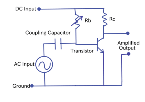
The circuit shown in the above figure is that of a Common-Emitter class A amplifier. Aha! so you can relate it with the general amplifier whose working you already understood in the beginning of this article. Yes, it’s very much the same with some minor changes which I will describe now. First of all the biasing resistors R1 and R2 are replaced by a single variable resistor R(b). R3 is renamed as R(c). R4 and bypass capacitor are fired from their job and are unemployed here. The working principle is same as the general amplifier, already explained well earlier. The Q point that slides in the load line otherwise is brought to it’s centre by adjusting the R(b).
![]()
The above model shows the load line with Q point at it’s centre. V(CEQ) is pretty much the same as V(CE) in terms of it’s behaviour, with the only difference being that it’s more of a specific kind of value than rather being a range of values. The same is true for I(CQ) and I(C) as well.
Characteristics of Class A Amplifier
It’s a low distortion type amplifier having very low efficiency but high gain. When there’s a cut-off in the transistor, the Collector-Emitter region behaves as open while in case of saturation the same Collector-Emitter region behaves as short.
Calculations in a Class A Amplifier
The biasing base current is given by the formula
I(B) = (DC Input Voltage – V(BE))/R(b)
I(C) = I(B) × DC current gain
V(CE) = DC Input Voltage – ( I(C) × R(c) )
Voltage gain = V(out)/V(in)
Applications of Class A Amplifier in Real World
- Voltage amplifier.
- Current amplifier.
- Power amplifier.
Tanmay Dasgupta is Working as a Freelance Technical YouTube Video Creator and Blogger for EFY Group. He strongly believes that Technology should be useful and should help in solving human problems or challenges. He is passionate about Core Electronics, Robotics and Cardboard modelling.

Very insightful and helpful article.
Thanks for sharing.
Thank You for your feedback.
Very helpful , thankyou …
Hi Aruna, you are most welcome.
thanks for all, its helpfull
You are most welcome.
Good article, useful for beginners, however, I would mention one thing, important to understand for beginners (I’ve seen misunderstanding a number of times on this).
At the end of the article, you show the formula:
I(C) = I(B) × DC current gain
which is perfectly fine mathematically but makes no sense physically as there’s no way to control the I(B).
It is important to explain that I(B) is a “parasitic”, unwanted component that we can calculate as:
I(B) = I(C) / DC current gain
Almost the same thing, but now it’s got the practical meaning.
Cheers,
Valery
Hello, good article. But i still have some questions.
-The biasing resistors, which are R1 and R2, are they calculated, so that, the base sees a voltage of e.g 0.7v when no signal is applied?