The trend of the worldwide market today still reserves about 80% of sales share for traditional ICE (Internal Combustion Engine) vehicles, while the remaining 20% includes overall xEV cars (all types of Hybrid and Electric Vehicles), where one of the most important sub-segments is the Mild Hybrid system.
The Mild Hybrid platforms, in fact, are already a concrete alternative to the traditional car architecture as they satisfy the demand for greater power availability while keeping the overall costs of the system low thanks to the following features:
- faster acceleration after a stop for the integration of the electric traction;
- higher fuel efficiency with start and stop systems;
- lower emissions thanks to turbocharger systems;
- greater safety than high voltage bus solutions in case of maintenance and failure events.
The ST POWER STripFET 80V – 100V devices with the F7 series already AEC-Q101 qualified and new automotive prototypes under development show good switching performance and efficiency with the adequate ruggedness to meet all automotive requirements. The MOSFETs are the right solution in terms of high frequency emission immunity for 48V to 12V DC-DC power conversion.
DC-DC Conversion in Mild Hybrid Architectures
The DC-DC converter used in Mild Hybrid vehicles transfers some of the energy stored in the main 48V lithium-ion battery to the 12V lead acid battery to keep it charged and serve low power loads and info-entertainment systems. This converter also allows a bidirectional power flow, as in some cases the 12V battery can partially recharge the 48V battery to provide the car with minimal range to the nearest service center.
This converter usually covers the following technical specifications:
- 2kW to 3.3kW output power in buck mode and up to 1.5kW in boost mode;
- output current about 250A;
- 12V – 14V output voltage;
- input voltage from 24V to 56V;
- efficiency greater than 93%.
The schematic of a multi-phase DC-DC buck converter is shown in Fig. 1.
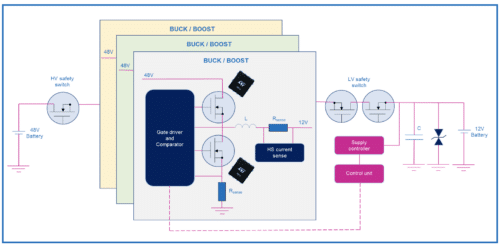
Fig. 1. Schematic of a multi-phase DC-DC buck converter.
The DC-DC converter is a power module consisting of:
- MOSFET half-bridge (HB) driven by a gate driver with an internal comparator for current sensing;
- HV safety switch used for the main 48V battery to protect and disconnect the system in case of faulty events; this switch is usually made up of parallel 80V MOSFETs with big die size, low static drain-source on-resistance (RDS(on)) and high current capability;
- LV safety switch to disconnect the 12V service battery, consisting of several parallel branches of two 40V back-to-back MOSFETs with very low RDS(on);
- control unit which synchronises, activates and regulates the interaction and activation of the phases according to the load level and also defines the shutdown of the system in the event of dangerous transition phases;
- additional protections against overcurrent events of the single phase and output overvoltage conditions due to battery disconnection.
In this topology, the high side (HS) MOSFET is optimized for the switching performance and noise of the converter affecting the efficiency at light loads, while the low side (LS) device is optimized to minimize the conduction losses, thus boosting the efficiency at heavy loads.
Therefore, the main features of the HS and LS MOSFETs in a 48V to 12V DC-DC converter can be summarized as follows:
- drain-source breakdown voltage (BVDSS) from 80V to 100V;
- gate threshold voltage (VGS(th)) with standard level;
- static drain-source on-resistance (RDS(on)) lower than 7.0mΩ for the HS MOSFET and 3.5mΩ for the LS device;
- total gate charge (QG) very low for the HS MOSFET;
- reverse recovery charge (Qrr) low for the LS MOSFET;
- ST’s PowerFLAT 5×6 package in case of MOSFETs connected in parallel and H2PAK package (2 leads or 6 leads) for a single device.
The switching losses (PSW) of the HS MOSFET are defined by the following equation (Eq. 1):

where:
- VIN is the input voltage of the DC-DC converter;
- IOUT is the current on the load;
- fSW is the switching frequency of the converter;
- QG,SW = Qgd + Qgs is the amount of charge required to turn on the MOSFET (equal to the sum of the gate-drain charge Qgd and gate-source charge Qgs);
- IGATE is the gate current of the MOSFET.
The conduction losses (PCOND) of the LS MOSFET can be calculated with the following equation (Eq. 2):
![]()
where:
- RDSon[T] is the on-resistance of the MOSFET at the operating temperature T;
- IDis the MOSFET drain current;
- D is the duty cycle of the converter.
The best compromise between minimizing the switching losses and optimizing the conduction losses defines the selection of a low on-resistance (RDS(on)) for the LS MOSFET and a low gate-drain charge (Qgd) for the HS MOSFET. This balance has a strong impact on the efficiency of the system and electromagnetic interference (EMI) noise emission.
Experimental Results
The STPOWER STripFET F7 automotive 80V – 100V MOSFETs are optimized for the sensitivity to the Miller effect and softness of the capacitance ratio (Crss / Ciss) compared to the previous series devices, as shown in Fig. 2.
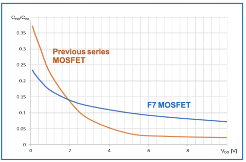
During the free-wheeling phase, the drain-source voltage (VDS) of the MOSFET is clamped to the forward on voltage (VSD) of the body drain diode. At transient turn-off, an increase in the VDS voltage occurs and the capacitance ratio plays a key role. Thanks to the soft trend and low initial value at almost VDS = 0V, the Crss / Ciss ratio provides the proper immunity to the Miller effect and contributes also to minimize the subthreshold conduction of the MOSFET and then the sensitivity to the EMI.
The main contribution to the EMI emission is linked to the reverse recovery charge of the body drain diode and its softness in the snap back (Fig. 3).
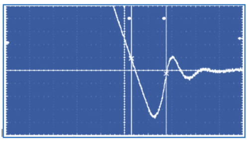
Experimental data show that the return to zero current for the body drain diode of STripFET F7 MOSFETs is quite soft producing only a few oscillations, thus limiting the high frequency emissions.
The automotive 80V – 100V MOSFET prototypes manufactured with the new technology offer, in addition, a good switching behavior with smoothed spikes of the VDS voltage and very short times for the oscillations. In a DC-DC converter for Mild Hybrid systems, the measured switching waveforms for both LS MOSFET and HS MOSFET at fsw = 250kHz, are reported in Fig. 4.
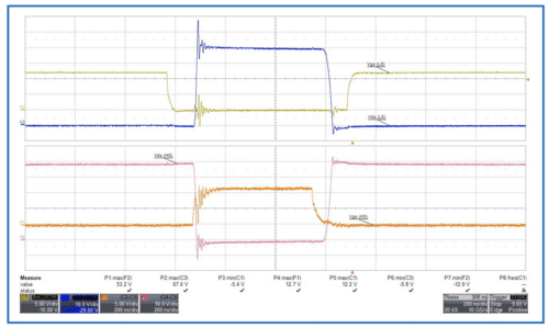
The above figure shows that the maximum spike of the VDS voltage in the LS MOSFET is only 52V (dark blue trace).
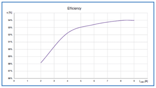
With the new MOSFETs, the measured efficiency of the DC-DC converter reaches 94%, as shown below (Fig. 5).
The efficiency of the converter is also affected by the reverse recovery charge of the body drain diode of the LS MOSFET and the new technological evolution provides for significant improvements even at high rates of change of the recovery current flowing to the body diode (di/dt), as shown by the measured recovery waveforms in Fig. 6.
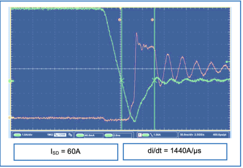
The real current flowing in the diode is 10 times greater than that shown in Fig. 6 because a current transformer was used for the current acquisition at ISD = 60A.
This recovery current also heavily determines the emission rate of the converter as it is the main source of high frequency noise due to oscillations as the current returns to zero. Near-field emission measurements highlight the EMI immunity of the new MOSFET prototypes and compare the emission rate with F7 devices. The experimental emission spectrum is shown in Figs 7 for the LS MOSFET and Fig. 8 for the HS MOSFET in a HB topology, when the devices switch at a current of approximately 15A.
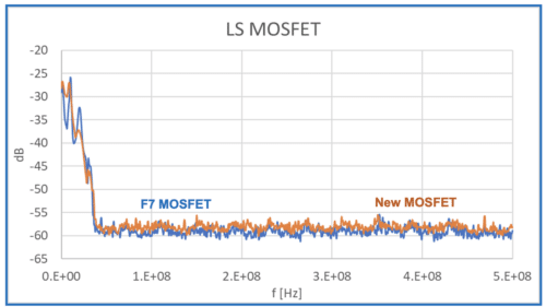
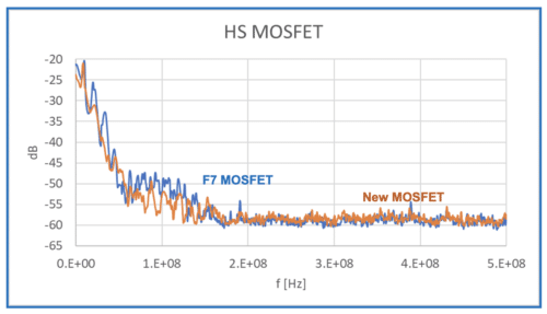
Both pictures show a higher emission rate value at lower frequencies corresponding to the switching conditions of the application, while at higher frequencies above 1MHz in the HS position the new technology prototypes show slightly lower emission rates than equivalent F7 devices in the same board and working conditions (switching frequency, current level and biasing voltage).
Conclusions
For Mild Hybrid systems, the new technology prototypes guarantee an increased efficiency for the DC-DC converter thanks to the improved switching behavior and reduced losses. In addition, they still maintain the good body drain diode performance for reverse recovery charge and softness like the STripFET F7 MOSFETs, helping to minimize high frequency radiated emissions. This is one of the best and well recognized features in any topology for automotive applications with power conversion and motor control.
References
[1] Z. Amjadi and S. S. Williamson, Power-Electronics-Based Solutions for Plug-in Hybrid Electric Vehicle Energy Storage and Management Systems, IEEE Transactions on Industrial Electronics, vol. 57, no. 2, Feb. 2010.
[2] E. A. Jones, M. de Rooij and S. Biswas, GaN Based DC-DC Converter for 48V Automotive Applications, IEEE Workshop on Wide Bandgap Power Devices and Applications in Asia (WiPDA Asia), Taipei, Taiwan, 23-25 May 2019.
[3] N. Mohan, T. M. Undeland, W. P. Robbins, Power Electronics Converters, Applications and Design, 2nd edition J. Wiley & Sons NY 1995.
[4] S. Musumeci, A. Tenconi, M. Pastorelli, F. Scrimizzi, G. Longo, C. Mistretta, Trench-Gate MOSFETs in 48V Platform for Mild Hybrid Electric Vehicle Applications, AEIT International Conference of Electrical and Electronic Technologies for Automotive, Nov. 2020.
[5] E. Armando, S. Musumeci, F. Fusillo, F. Scrimizzi, Low Voltage Trench-Gate MOSFET Power Losses Optimization in Synchronous Buck Converter Applications, 21st European Conference on Power Electronics and Applications (EPE ’19 ECCE Europe), Sept. 2019.


