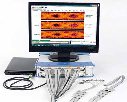
High-speed Flash memory and solidstate drives (SSDs) have become a staple diet of all consumer electronics devices from smartphones to laptop computers. It is almost impossible to imagine a gadget without high-speed storage. Thus it is obvious that a vital part of the production and testing of these devices is to ensure that their memory matches in speed with the rest of the device
Ashwin Gopinath

Arecent survey by the International Electronics Manufacturing Initiative (iNEMI) asked test engineers in the electronics industry what their biggest problems were while testing circuit boards.
Of the eleven possible problems listed, characterising and testing memories soldered to circuit boards was among the top three. Memory test topped the list of prevalent problems along with ‘lack of access to test points’ and ‘the need to perform debug/diagnostics on board failures.’ Clearly, the ability to thoroughly characterise, test and diagnose problems with soldered-down memories is one of the most pressing problems in the industry.
When memory speeds were not as high as today’s communication protocols’ and over memory buses were not as complex, performing static shorts and opens testing on memory interconnects might have sufficed. Today, signal propagation through passive devices such as capacitors and signal integrity on high-speed traces to memory must be validated and characterised for an open data window. Often this data window demonstrates sensitivities to clock jitter, temperature, electrical noise as well as the level and stability of the voltage.
One of the several factors that have exacerbated the difficulties in memory testing is the complexities of these buses. Many of the prominent memory buses, like the various generations of double data rate (DDR) memory, have achieved extremely high data transfer rates at the expense of simplicity. Indeed, the difficulties in testing memory buses have only been exasperated by each successive generation’s high transfer speeds.
Under the hood of memory testing
All memory tests are based on writing to and reading from the memory. Test reads and writes conducted from the board’s functional or normal memory access unit in a normal operating manner can be referred to as functional memory tests. Usually, functional memory tests can prove out the design or functionality of a given memory architecture, but these may not be able to detect or even diagnose manufacturing or assembly defects.
Most manufacturing memory tests are algorithmic and structural pseudo-functional tests. The most prevalent form of an algorithmic pseudo-functional memory test is memory built-in self-test (MBIST). MBIST implies that the test is implemented on-silicon or provided by an algorithmic test instrument embedded within a memory test system.
Since memory testing is an altogether different field of operation, parameters tested and methods for testing vary a great deal.
Explaining the memory test, Abhay Samant, marketing manager, National Instruments, says, “A memory test consists of testing the various components of the memory, including testing for functional performance of the address and data lines, and timing tests. The lines are tested using various patterns such as marching ones or pseudo-random values. The values are then read back and compared against expected data for errors. For conducting functional tests on the memory tester, all lines on the memory are tested with sequences such as moving ones, random moving inversion bits, or a random number sequence.”
Sanchit Bhatia, digital applications specialist, Agilent Technologies, adds, “DDR is the most popular high-speed memory standard. It is defined by the Joint Electronic Devices Engineering Council (JEDEC) specifications. The JEDEC specifications have strict jitter requirements for the clock and strict signal integrity requirements for all signals. To qualify, the clock must pass a long list of jitter tests and data signals should pass a long list of timing tests. With automated DDR software, jitter measurements can be carried out more efficiently and effectively.”
Roy Chestnut, product line manager at Teledyne Lecroy, chimes in, “DDR signalling is a parallel data bus that requires validation of a variety of DDR-specific physical-layer measurements (slew rate, amplitude, overshoot, etc) that are closely defined by the JEDEC standards. These parametric measurements are not standard in oscilloscopes, and it would take users a long time to set up the oscilloscope to make them. Additionally, parallel nature of the DDR bus requires close timing coordination of the various clock, strobe and data signalling. These timing measurements in a variety of test conditions are also automated. Lastly, a variety of fairly standard clock jitter tests are also automated. We have products that focus on command and address timing between the system memory controller and the memory.”
Challenges
In the broadest sense, memory testing takes place over the entire life-cycle of a system, beginning with board development or design, moving into production and culminating in post-production stages such as field service. The cycle then repeats when a memory test is performed during the next generation of board design. During each phase in the life cycle, the objectives and goals of memory test differ and the memory test process itself is typically referred to differently, according to the objectives of that particular phase.


