So what comes to your mind when you hear the word ‘Intel’? Definitely, a manufacturer of all your celeron’s, pentium’s, dual cores, core i’s, and other micro-processor chips, right? The pace dictated by Moore’s Law has required numerous innovations and as a result of which the ‘Sponsors of Tomorrow’ introduced a three dimensional transistor technology, which is basically, Tri-Gate transistors on its 22 nm logic technology.
Important Turning Point in Transistor Technology
In 1947, the first transistor was demonstrated at Bell Laboratories. Silicon was first used to produce bipolar transistors in 1954, but it was not until 1960 that the first silicon metal oxide semiconductor field-effect transistor (MOSFET) was built. The earliest MOSFETs were 2D planar devices with current flowing along the surface of the silicon under the gate. The basic structure of MOSFET devices has remained substantially unchanged for over 50 years.

Continued optimization and manufacturability studies on 3-D transistor structures was on at research and development organizations in leading semiconductor companies. Some of the process and patent development has been published and publicly shared, and some remained in corporate labs. The International Technology Roadmap for Semiconductors (ITRS) drives the research investment interests of the semiconductor industry, which is coordinated and published by a consortium of manufacturers, suppliers, and research institutes.
The ITRS defines transistor technology requirements to achieve continued improvement in performance, power, and density along with options which should be explored to achieve the goals. The ITRS and its public documentation captures conclusions and recommendations regarding manufacturing capabilities like strained silicon and High-K metal gate, and now the use of 3-D transistor technologies to maintain the benefits of Moore’s law. Based on documents produced by the ITRS and an examination of academic papers and patent filings, research into 3-D transistor technologies has grown dramatically in the last decade.
The Triggers That Threw Spotlight on 3-D Transistors
Two important pronouncements that have occurred in the last two years that have propelled the 3-D transistor structure into the industry spotlight, and into a permanent place in the technology story of MOSFET transistors are 1) The first announcement by Intel Corporation on 4th of May, 2011, about their Tri-Gate transistor design that had been selected for the design and manufacture of their 22 nm semiconductor products. 2) The second announcement was the publication of ITRS technology roadmaps, with contributions from many other semiconductor manufacturing companies that identified 3-D transistor technology as the primary enabler of all incremental semiconductor improvement beyond the 20 nm or 22 nm design node.
So Exactly How Small is 20 nano-meter?
Each and every micro-processor manufactured today is made of millions, or even billions, of tiny electrical components called transistors. Over time, in accordance with Moore’s law, transistors have been getting smaller and smaller and because of which, computing and communication devices continue to get smarter, faster and highly efficient.
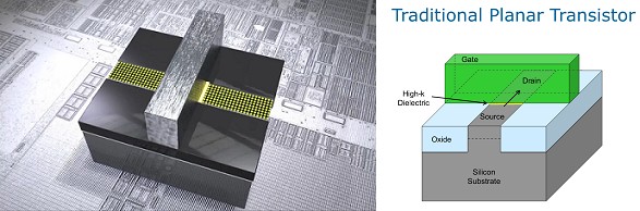
Intel believes that keeping up with Moore’s Law has never been exactly easy. Especially for 22 nanometers, Intel claims that it became clear early on that continued shrinking was not going to give the expected benefits without some radical redesign. After a decade of research and development, taking advantage of the work of Hisamoto and others in FinFET development and optimization, Intel invented the solution. For the first time in history, the transistor has officially entered the 3rd dimension. Image 1 shows what a 3D transistor looks like.
In fact, there are more than a billion transistors on this single chip which, unfortunately, are far too small to be seen with the naked eye. Now imagine yourself 20,000 times smaller! To give you a point of reference, right now, you are even smaller than a human hair. But you would actually still be far too large when compared to a 22 nano-meter transistor for a meaningful imagination. You actually need to be 100 nano-meters tall or about 20 million times smaller than your actual size. At this scale, you are about the right size to literally see, demonstrate some of the attributes and functions of a single, modern transistor out of those millions of transistors inside the 3D transistor chip. Well, since there’s no such shrinking device as yet, let us just consider the figures below as transistors models and understand.
But first, what are 2-D transistors?