Uncover the driving forces behind the semiconductor revolution—how AI slashes human error, unearths untapped revenue streams, and underscores the pivotal role of customisation with domain-specific chipsets.
The surge in demand for artificial intelligence (AI) and the Internet of Things (IoT) devices is reshaping how we interact with technology and the world around us. From smart trackers in our watches to intelligent thermostats in our homes, the application of artificial intelligence (AI) is permeating every aspect of our lives. A consumer survey predicts that by 2030, we will be surrounded by more than 350 billion AI IoT devices, underlining the rapid growth in demand for these devices.

While the proliferation of AI IoT devices is impressive, it also raises questions about the role of AI in improving our lives and the potential for human error in these technologies. In this article, we will explore the key trends in AI applications, the need for increased computational power, and the driving agents behind this revolution in the semiconductor industry.
AI Applications and Reducing Human Error
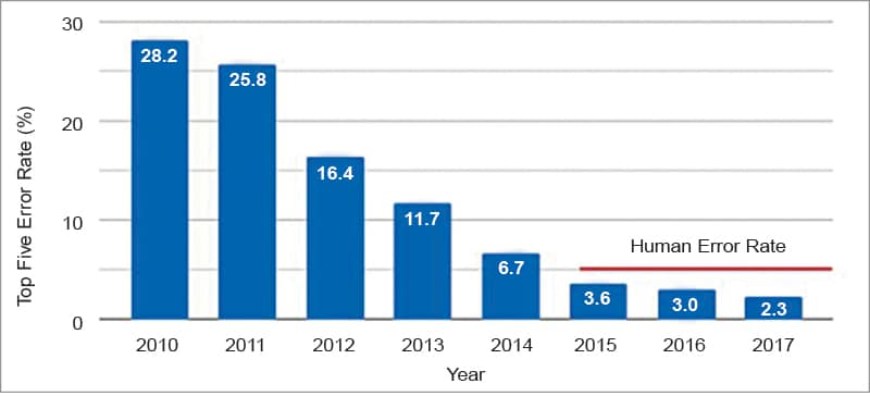
The primary goal of integrating AI into IoT devices is to enhance their capabilities and reduce human error. AI can provide more accurate results than the human eye or persistence in various applications, such as image recognition. For instance, thanks to machine computing power, Google’s image recognition application significantly reduced human error rates when AI was utilised. As a result, there is a growing need for complex system-on-chip (SoC) architectures to support these AI use cases. These architectures must evolve to accommodate single-threaded applications, OpenCL support, benchmarking, multi-threaded networking applications, and image recognition.
In networking applications, focus lies in leveraging network function processors to enhance system performance. One significant aspect that has been emphasised is security, primarily due to the vast data transmitted between edge devices and cloud services. We must ensure the integrity and authenticity of this data along its journey.
We are actively implementing robust computing mechanisms within the communication channel to achieve this. These mechanisms are designed to verify and validate data integrity at both the edge and cloud endpoints. Ensuring the data’s accuracy is paramount, guaranteeing that the information transmitted aligns with the intended content.

| Key driving agents in semiconductor evolution |
| Several key driving agents have played significant roles in shaping the semiconductor industry over the years: Technology shift in AI compute requirements • The semiconductor industry experiencing a technology shift due to rising demand for AI applications • OEM manufacturers and chip design teams engaged in application benchmarking to assess computational power capabilities • AI integration into daily life necessitates hardware adaptation to meet increased demands Surge in demand for sub-micron compute devices • Computers are shrinking in size while computational demands are on the rise, creating a paradox • Developing sub-micron computing devices and manufacturing technologies is essential to address this challenge • Industry must support smaller yet more powerful devices, reduce costs, and ensure reliability The role of more (reliability, stability, and power efficiency) • Semiconductor engineers face reliability, stability, and power consumption challenges in sub-micron technology • Increasing the transistor count on chips necessitates maintaining high-reliability standards • Ensuring reliability is vital for the seamless operation of AI-powered devices These driving agents continue to shape the semiconductor industry, with advancements in chip design, manufacturing, and applications leading to ever more powerful and efficient electronic devices. |
The pursuit extends to fulfilling the computational demands associated with image recognition. This necessitates efficient computing resources to analyse and process visual data, further enhancing the capabilities and value of our networking applications. Companies like Nvidia are at the forefront of providing the necessary computational power to meet these demands.
Also Check: Application of Artificial Intelligence in the Manufacturing Sector
Automation in the Semiconductor Lifecycle
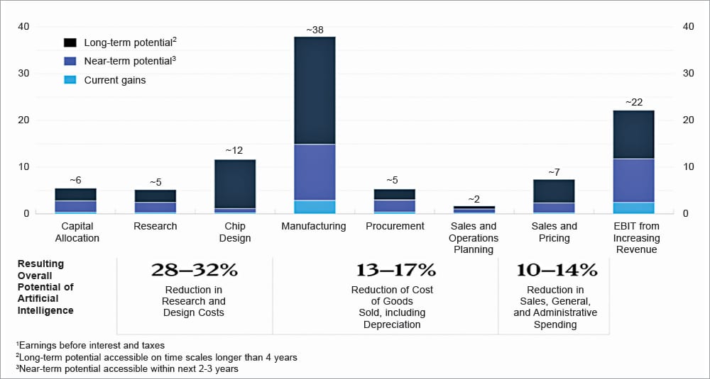
Automating the semiconductor lifecycle is another crucial aspect of the AI revolution in the industry. McKinsey’s research suggests that AI could generate $85 billion to $95 billion in revenue over the long term, highlighting the untapped potential of AI-driven automation in semiconductor manufacturing. As AI techniques become more advanced, semiconductor companies embrace them to streamline processes and improve operational efficiencies.
The AI revolution is reshaping the semiconductor industry in profound ways. The demand for AI IoT devices is driving the need for increased computational power, sub-micron compute devices, and more reliable semiconductor designs. Additionally, the automation of the semiconductor lifecycle through AI promises significant revenue potential. As we continue integrating AI into our daily lives, the semiconductor industry will play a pivotal role in supporting these technological advancements, ultimately shaping the future of our interconnected world.
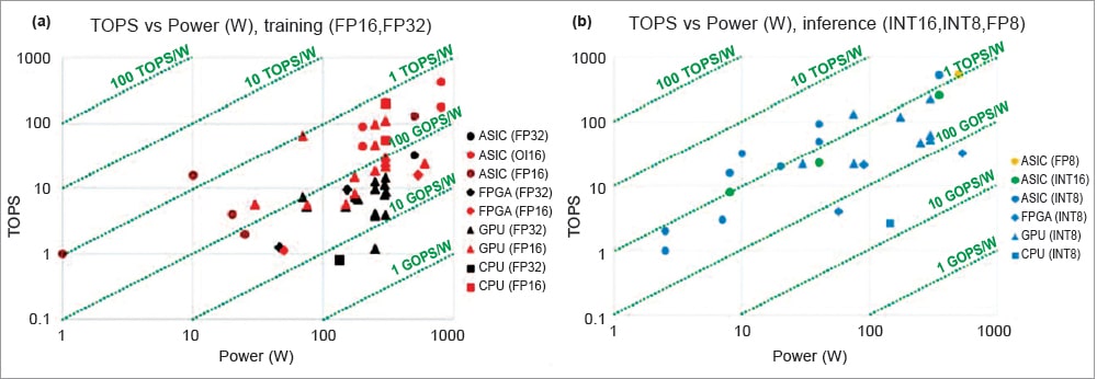
The semiconductor industry is no stranger to innovation and adaptation. To meet the demands of AI applications, it’s crucial to assess whether our chipsets can support various AI tasks effectively. Benchmarking is pivotal in this exploration, comparing AI accelerators across different chipsets by measuring ‘TOPs’ (tera operations per second).

TOPS is a Simplifying Metric
TOPS tells you how many computing operations an AI accelerator can handle in one second at 100% utilisation. In essence, it looks at how many math operation problems an accelerator can solve in a very short period.
What is interesting to note is that scalability in chip design is not always linear. Increasing computational power by merely adding more cores or capacity doesn’t guarantee a proportional boost in performance. This highlights the importance of rigorous architectural exploration and benchmarking operations to ensure that AI applications can be handled efficiently by hardware.
Undeniable Trend in AI Hardware Design
Linear scalability is not as straightforward as it may seem. Simply increasing system-on-chip (SoC) capacity and compute power does not necessarily equate to a proportional boost in computational capability. This vital message underscores the need for a deeper exploration of system architecture and comprehensive benchmarking operations to ensure our hardware effectively handles AI applications.
Initially, the prevailing wisdom among system designers was that expanding compute power primarily involved ramping up the number of CPUs and cores to achieve maximum performance. However, contemporary benchmarking efforts have revealed that this approach does not yield a direct and flawless linear scaling. Increasing the number of cores, while beneficial to a certain extent, encounters limitations related to power consumption and other systemic architectural constraints.
To meet the demands of AI applications, it is imperative that we delve into other facets of system design. This shift in perspective is crucial to facilitate the seamless transition of our hardware to accommodate diverse use cases. For many of us in this field, this shift in thinking is of personal interest. It brings into focus the critical importance of application benchmarking in assessing the overall system design.
The quest for optimal solutions extends beyond mere processing power and touches upon the intricacies of power efficiency, architectural design, and the diverse needs of AI applications. In this journey, time to market remains a significant consideration. Complex application benchmarking has become an integral part of our strategy as we strive to bridge the gap between hardware capabilities and the evolving demands of AI applications. Through these efforts, we aim to ensure that our hardware is not just keeping pace but leading the way in the dynamic realm of AI technology.

Customisation and Domain-specific Chipsets
Traditionally, semiconductor designers aimed to increase compute power by adding more general-purpose CPUs and cores. However, as benchmarking has shown, there are limits to this approach, constrained by factors like power consumption and system architectural limitations. This realisation has led to a shift towards domain-specific chipsets.
Today, chipsets can be designed to serve specific domains or applications. Rather than a one-size-fits-all approach, these domain-specific chipsets can be tailored to the unique requirements of different applications, such as web browsing, minimal applications, multimedia, image recognition, and more. This customisation allows chipsets to be more efficient and cost-effective, meeting the specific needs of each application.
One of the most exciting developments in semiconductor design is the emergence of software-defined hardware. This paradigm shift recognises that while general-purpose chipsets have their place, the future lies in custom, adaptable chips designed for specific tasks.
Software-defined hardware allows chip designers to create modules that can be activated or deactivated depending on the application’s requirements. This flexibility ensures that the chip remains power-efficient and capable of delivering high performance for the intended task. It is a revolutionary approach that addresses the dynamic needs of the modern AI landscape.
Beyond chip design, AI is making significant inroads into the entire semiconductor lifecycle. McKinsey’s research suggests that AI can play a crucial role in various stages, from capital allocation and product portfolio definition to chip design and supply chain management.
AI-driven automation promises to streamline processes, improve operational efficiencies, and reduce costs. For example, Google’s open chip architecture leverages AI to design chipsets, demonstrating the potential of AI in semiconductor design. Additionally, AI can optimise supply chain operations, mitigating issues like the supply chain disruptions experienced during the Covid-19 pandemic.
The semiconductor industry is on the cusp of a revolution driven by AI and customisation. As the demand for AI-powered devices continues to grow, semiconductor designers must adapt to meet the diverse needs of different applications efficiently. Software-defined hardware, domain-specific chipsets, and AI-driven automation are key trends that will shape the industry’s future.
Recognising the strategic importance of AI and talent development, semiconductor companies are embracing AI as a top priority. The International Technology Roadmap for systems and devices (IEEE) is also actively contributing to the ecosystem’s development. The semiconductor industry’s transformation is inevitable, and those who harness the power of AI and customisation will thrive in this new era of semiconductor design and technology.
The semiconductor industry is in the midst of a transformative era, driven by the integration of AI and the growing demand for customisation. In a recent discussion, industry experts explored the various facets of this revolution, from custom chipsets to software-defined hardware and the role of AI in reshaping semiconductor design and development. In this article, we will take a closer look at the insights and innovations shared during this enlightening conversation.
AI’s Role and Customisation with ASICs and Domain-specific Chipsets
Application-specific integrated circuits (ASICs) and domain-specific chipsets, as the name suggests, are designed with a specific application or use case in mind. These chips are tailored to excel in their intended application, whether AI for autonomous vehicles or industrial automation.
What is noteworthy is that these ASICs are not one-size-fits-all solutions. Instead, they are finely tuned to meet the unique requirements of each application, resulting in improved efficiency and cost-effectiveness. This move towards customisation is changing the game in semiconductor design, allowing companies to offer specialised chipsets that cater to diverse industries and applications.
The software-defined hardware challenges the traditional approach of fixed hardware configurations. Instead, it introduces flexibility by enabling modules within a chip to be activated or deactivated depending on the specific application’s needs.
For example, consider a Tesla car. Customers can purchase a base model and then choose to enable additional features or functionalities as needed. These features are already present in the hardware, but they can be unlocked through software activation. This approach allows for greater adaptability and efficiency in hardware usage.
AI is making its mark throughout the semiconductor lifecycle. One notable application of AI is in creating knowledge bases and chatbots to aid in post-silicon ramp-up. Semiconductor engineers face the challenge of rapidly acquiring diverse skill sets as they work on chips for different applications. To streamline this learning process, companies are using AI-driven chatbots to provide engineers with quick access to training materials, data, and insights, helping them ramp up more efficiently.
In the pre-silicon phase, AI is proving invaluable in the realm of safety simulations. In the automotive industry, safety is paramount, and AI simulations are being used to test and verify chip functionality in critical safety scenarios. This ensures that chips meet the stringent safety standards for applications like autonomous vehicles.
Untapped Revenue Potential
By integrating AI into various aspects of the semiconductor process, companies can improve operational efficiencies, reduce costs, and create new revenue streams. For instance, AI can optimise capital allocation, enhance product portfolio definition, assist in chip design, and streamline supply chain management.
The McKinsey and Company study suggests that embracing AI in semiconductor development could yield significant returns, with potential savings ranging from 28% to 32% of design costs. These findings underscore the compelling business case for AI adoption in the semiconductor industry.
The semiconductor industry is profoundly transforming, with AI and customisation at the forefront of innovation. From ASICs and domain-specific chipsets to software-defined hardware and AI-driven automation, the industry is embracing change to meet the demands of a dynamic and interconnected world. As AI continues to reshape semiconductor design and development, companies that leverage its power and adapt to the evolving landscape will be well-positioned for success in this exciting era of semiconductor technology.
Field-programmable gate arrays (FPGAs) offer developers the ability to define custom applications and modules within the chip, providing flexibility and adaptability for iterative development and testing. On the other hand, the SoC approach fabricates chips specifically for a particular application, optimising hardware for efficiency and performance. Advancements like five-nanometre technology in SoCs enable more complex computations.
The integration of AI into the semiconductor industry is further driving innovation, optimising hardware, enabling software-defined upgrades, and improving post-silicon knowledge bases. These advancements promise an exciting future for custom applications and chip design.
It becomes evident that we are on the brink of a transformative era. The demand for AI IoT devices is propelling the industry to innovate at an unprecedented pace, requiring increased computational power, domain-specific chipsets, and software-defined hardware. AI’s integration into the entire semiconductor lifecycle promises operational efficiencies and significant cost savings.
The future of semiconductor design and technology is being shaped by AI and customisation, and those who adapt will thrive in this dynamic landscape. As we continue to witness the seamless integration of AI into our daily lives, it is clear that the semiconductor industry holds the key to unlocking the limitless possibilities of a more interconnected and intelligent world.
This article is based on a tech talk session at EFY Expo 2023, Delhi, by Balvinder Khurana, Senior Engineering Manager System Validation, NXP. It has been transcribed and curated by Akanksha Sondhi Gaur, Research Analyst and Journalist at EFY.


