Increase in the complexity of electronic boards shows manual inspection may not be a viable option. With the marketplace now requiring high quality, no-error products, there is a strict need for reliable fast methods. One of the effective solutions is to integrate AOI in your electronics test strategy
Automatic optical inspection (AOI) is a key technique used in manufacturing and testing of electronics printed circuit boards (PCBs). It enables fast and accurate inspection of electronic assemblies, thus ensuring production of high quality of boards without defects. This technique usually comes at the stage just after the soldering process to find and fix faults, especially in the solder and assembly area. In this way of rapid response, defects are recognised quickly and rectified before too many boards are built with the same errors.
Not only identifying errors and pausing production of defective boards, AOI provides data needed to improve the performance of the entire SMT process. AOI uses various techniques like template matching or pattern matching to check the quality of a board. It compares the captured image with the image of a ‘golden board’—an ideal board that is of acceptable quality and standard, stored in the database. It can be used to adjust and improve the quality of manufacturing without stopping the process. The need for a dynamic SMT inspection equipment has driven manufacturers to connect their equipment and process data to enable smart, adaptable functioning of AOI machines.
What an AOI machine does
These inspection systems use visual methods to monitor PCBs to detect various surface defects like nodules, scratches, and stains and other dimensional defects by in-circuit testing (ICT), such as open circuits, shorts, discontinuity, and thinning of the solder. They can also detect incorrect components, missing components, and incorrectly placed components.
An AOI machine uses optical light energy to capture and analyse images of PCBs to verify the assembled electronic components, including presence and position, soldering (solder joints and bridges), polarity, marking (like inscription, signs, colour), flux deposits, microcracks, and subsurface defects. It performs with the help of illumination, CCD image system and processing software, machine vision camera, AC servo control, XY workbench, image processing system, and other actuating parts.
Illumination system
While older AOI machines used fluorescent, incandescent, ultraviolet, or infrared lights, today’s machines use smart red, green, white, or blue coloured light emitting diodes (LEDs). LEDs are preferred for their ability to provide a stable form of lighting. With efficient control over the light, LEDs provide uniform illumination.
Along with the type of lighting, the orientation of the light source is also important. Machine vision camera systems assist the illumination system with effective lighting control and intensity adjustments to capture the entire PCB in audit.
CCD image system
CCD is a charge coupled device, a semiconductor element that converts images into digital signals. An AOI system uses a CCD camera for imaging. The system consists of a lens, an image sensor, and image processing tools.
The image sensor forms the heart of the camera. The photon energy captured by the camera lens and the individual pixel information is absorbed by the respective photocells in the sensor. The camera sensor converts incoming photon energy into electrical charges, which are further processed to generate images. The image processing system is the key for extracting the information through images in any application.
In AOI, the processing of images takes place externally through the PC based system supported by various processing tools. The AOI machine’s imaging resolution defines the amount of detail it can identify and capture, and hence it is a key factor that affects the inspection accuracy and inspection speed.
Machine vision camera
The image capture takes pictures for analysis. This is assisted by one or more high-definition cameras installed within the AOI to focus or move under the software command. Recently, these cameras have been featured with higher frame rate to support faster scanning and generate more data. An efficient processing software is hence required to manage huge amount of data.
Resolution turns out to be an important aspect as it defines the field of view (FOV) that specifically shows the section in an image. A wider FOV would typically allow the product to be examined with lesser images. However, it takes more time to capture each image as the camera with more pixels leads to a lower frame rate. On the other hand, cameras with a narrow FOV have bigger pixels with higher frame rate.
Processing software
For an AOI machine to inspect a product, the data of an acceptable product must already be fed to the system. There are primarily two ways in which AOI machines are programmed. Image based programming uses scanned images of ‘golden board’ where references are created and accordingly automated. Algorithm based programming is the other method where the system generates its profile for the product by feeding product data to it.
Now, with all the elements working together, systematic outputs are obtained. Depending on the results, corrections are either made automatically or by human interference.
AOI challenges
While there have been great developments in the manufacturing of AOI machines over the years, many challenges still persist. Manufacturers are coming up with various solutions that are described below to tackle them.
Optical inspection
AOI systems were earlier based on 2D inspection technology where different grey levels for solder paste, solder joint, and component detection were inspected. Today, the 2D technology is being overtaken by 3D measurement solutions.
While many 2D AOI systems remain in use, the effort needed to keep this technology at a low level of escape and false-call rates is tremendously high. This is because the 2D systems work by comparing reference images. To help, some equipment manufacturers have added additional cameras and projectors to create quasi 3D or 2.5D technology, but it is still based on the same antiquated, inadequate comparison, or colour assessment.
AOI machines enabling both 2D and 3D imaging features along with other capabilities are being developed to provide extensive precision in the inspection process. Today, most AOI equipment has the capability to perform multiple tasks, reducing the time and expenses in the SMT process.
“To avoid faulty solder joints, defects, false calls, and costly rework, we may need easier 3D solder paste inspection as well as 3D AOI inspection,” says Olivier Pirou, Head, Product Management and Marketing at Mycronic, an AOI manufacturing company.
Most of the AOI solutions still offer a limited level of 3D coverage for components and solder joints. But a full 3D coverage is needed to identify defects. These full-coverage 3D AOI systems not only inspect common defects, such as missing or wrong components, but accurately provide true volumetric height, identify coplanarity, and lead-bridging issues.
Some 3D AOI solutions have used the multi-frequency shadow moiré technology. Unlike 3D AOI systems using a brightness threshold, the moiré technology uses the height threshold to extract critical body and the lead tip information. This data allows the AOI to provide reliable body and joint measurements with CAD dimensions. It can locate the body properly in the first stage of the inspection process.
However, 3D inspection systems also have disadvantages. This approach cannot check for printed part nomenclature, polarity marks, or colour. Even after using multiple digital projectors, shadowing may occur. Therefore, some additional programming may be required to train inspection components. Using 3D inspection can increase cycle times as projectors may need more time to project multiple fringe patterns needed for image processing. And lastly, machine costs are comparatively high as the technique is not yet mature.
Shadow problems
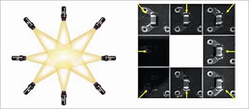
The shadow problem is inevitable even in 3D inspection machines. When various components are assembled on a board, some short parts like resistors may be shadowed by tall neighbouring components like connectors. This may lead to inaccurate 3D measurement results.
Many manufacturers use an 8-way projection mechanism shown in Fig. 1 that could possibly eliminate blind spots and construct a true 3D image by using multiple projectors.
Board warpage
Sometimes, on a warped board, pad positions defined by board CAD or Gerber files appear distorted. This may confuse conventional inspection systems and generate incorrect data. The board warp becomes a prominent issue during the reflow process because of high temperatures.
Creating new advanced algorithms can possibly address this challenge.
Inter-reflection and solder joint problems
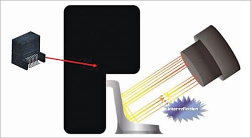
Inter-reflection is a common issue in most optical systems, where light itself becomes the source of information. In the PCBs, soldered and tinned components on assembled boards may have specular surfaces, which reflect some lighting back to the camera while creating strong inter-reflection with other lighting reflections. In such a case, some reflected light does not reach the camera and generates false signals that provide incorrect measurement details.
Some AOI systems today overcome this with the use of superior multi-view sensors. Using these multi-view sensors and advanced 3D image fusion algorithms, it is possible to obtain error-free measurements.
Measuring a solder joint is a complicated task as each solder deposit may vary according to the design and printing conditions. Specular reflections in these will not allow to detect solder defects.
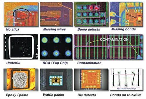
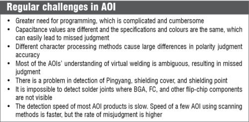
Apart from these challenges, more overlooked problems that lead to misjudgment and missed judgment are usually inevitable.
State-of-the-art inspection machines
With all that said about AOIs, let us have a look at some of the latest AOI machines.
Omron’s S10 series
It is a full colour system, offering a unique mix of general-purpose and application-specific solutions. S10 series enables flexible manufacturing, responds to shortages in manpower, and demands for higher quality production. Elimination of shadow and secondary reflection with 4-direction MPS projectors allows stable inspection of fine parts and enables visibility even at the connector solder joint.
Mycronic’s MYPro series 3D AOI system
This newly designed user interface with intuitive programming guidance and self-optimising process control algorithms ensures easy implementation of high-performance 3D AOI for any type of production mix or class by operators of any experience level.
Saki Corporation’s 3Di-LS2-CASE
It significantly reduces the number of false calls in the inspection of solder defects (non-wetting) that is difficult to achieve with conventional 3D-AOI technology, and dramatically improves the speed and accuracy of solder defect detection.
CyberOptics’s SQ3000+ multi-function system
The SQ3000+ multi-function system for inspection and metrology not only conducts AOI and SPI but claims to deliver in-line, full coordinate measurement (CMM) data in seconds. The new SQ3000+ offers a combination of high accuracy and high speed with an even higher resolution multi-reflection suppression sensor that inhibits reflection based distortions caused by shiny components and surfaces.
 Can AOI do it alone?
Automatic optical inspection works well in PCBs with clearly visible solder joints. However, many PCBs today are using other technologies, such as ball grid array (BGA) integrated circuits or chip scale packages (CSPs), where the solder joints are not visible. Such cases may need extended support with automated X-ray inspection (AXI) equipment that can check solder joints under components.
Manufacturers can consider ways to combine the inspection technologies rather than choosing between them, depending on the complexity of the PCB. Each of their advantages can be carefully balanced against cost to suit a particular production environment.
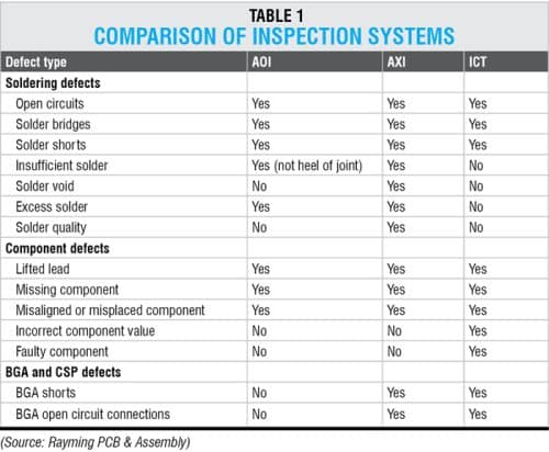 “AOI and AXI have been following the trend of most recent technologies to provide more performance for less cost. Another recent development is the portability of data between AXI and AOI systems from some suppliers. The ability to share libraries, inspection programs and statistical process control (SPC) data between AOI and AXI systems can greatly enhance machine usage and defect coverage. In addition, programming the systems of today is fast and intuitive. Operators are now able to quickly and easily create inspection programs and manage daily runtime operations with very little intervention. As a result, both high-mix and high-volume manufacturing lines can recognise immediate yield improvement and automated inspection results,” says Kevin Garcia, Applications Engineering Manager, Nordson YESTECH, an inspection equipment manufacturing company.
The advantages of current-day inspection systems over price and performance are becoming the driving force to handle dynamic manufacturing environments in giving successful yields.


