


Existing system-level exploration tools can provide early power, area and cost estimates, and allow what-if explorations across architectures, silicon IP choices and foundry processes. However, these tools need to be extended to serve stacked die implementations, package and manufacturing considerations, as well as provide some guidance on tradeoffs that system houses would have to make between cost, power and performance.
3D floorplanning. 2D floorplanning is complex enough in today’s giga-scale designs. Adding a third dimension makes floorplanning even more challenging. Since TSVs can be very large compared to logic gates (they add more wire length and extra coupling, which is mitigated by keep-out zones that add area), a TSV-aware 3D floorplanner must allocate optimised TSV resources with respect to logic gates.
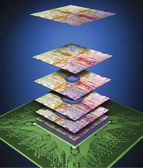
3D implementation. Synthesis, placement and routing for 3D ICs bring forth a number of new considerations. For example, there are new layout rules that may be driven by features on the adjacent die. The back-side RDL is a new layout layer. Given their size, TSVs themselves are a significant new layout feature. An implementation system that supports 3D ICs must be made ‘double-sided aware,’ taking into account both the top and bottom of each die. This may call for a new modelling and database infrastructure, TSV-specific tools and support for a variety of stacking styles.

3D extraction and analysis. Extraction and analysis is already challenging in a 32nm 2D scenario, but this design convergence is even more complicated with 3D ICs. Existing extraction and analysis tools must consider RLC parasitics for TSVs, micro-bumps and interposer routing. Also, they must be made 3D-aware. Timing, signal integrity, power and thermal gradients must be analysed across multiple dies and packaging taken into consideration.
Signoff raises new questions with 3D-IC stacks: When is the right time to sign off? What are the appropriate signoff points? Can design rule check (DRC) and layout-versus-schematics (LVS) run on the entire stack? Should and can timing be verified for the entire stack? Is there any crosstalk between dies? Finally, electromagnetic interference (EMI) is a potential concern for 3D ICs and a consideration for analysis tools.
3D DFT. Design for test (DFT) for 3D ICs is even more critical than for 2D ICs. While wire-bonded systems-in-package (SiPs) may have a few hundred interconnects, 3D ICs may have thousands. Even a single defective TSV can render an entire stack unusable. If individual TSVs have 99.9 per cent yield, at least one defective TSV can be expected in a stack of 1000 TSVs.
To provide test generation, the wrappers should support the internal testing of each die as well as all the inter-die interconnect logic and TSVs. In addition to the traditional fault models used for digital testing (stuck-at, transition, stuck-open, bridge faults), 3D ICs require specific interconnect fault models to test the TSVs and micro-bumps. For designers, this means that in addition to expanding EDA tools to be 3D-aware, they have to start thinking in 3D.
Joseph Sawicki, VP and GM, Design to Silicon Division, Mentor Graphics Corp., elaborates: “In the area of digital physical design (place and route), the challenge of 2.5D is mainly creating silicon interposer (SI) layouts. Interposer design must address pin-out, bump placement, support for 45-degree and tapered routing, and length matching to control timing and parasitic capacitance in passive interposers. Some modest extensions are needed to adapt IC P&R tools for this task.
“On the other hand, there are a variety of impacts when considering full 3D design, starting with floor planning and cell placement. Block partitions need to consider multiple constraints such as TSV location, connectivity, area and congestion when deciding how blocks will be realised on different dies. Placement needs to be done in three dimensions considering the vertical plane assignment of standard cell/macros to minimise wire length and via count. Clock tree synthesis and routing must try to minimise congestion using TSVs, and it is critical that clocking is balanced across planes as well across each die.”
According to Sawicki, for 2.5D, DRC and LVS verification challenges are relatively modest. Dies are developed/verified using the existing design and verification flows. Then the die interfaces, usually silicon interposers, are designed and verified using a similar flow with some enhancements to handle multi-die pin-out naming checks. Parasitic extraction tools are being enhanced to handle silicon interposers, front and backside metal layers, and inter-die coupling, which require new models for these elements. For full 3D (stacked die with TSVs), there are lots of new challenges such as thermal modelling (including the impact of IR drop), power network integrity, stress modelling, and modelling of the parasitic effects of TSVs interacting with each other and with transistors in active die areas.
