


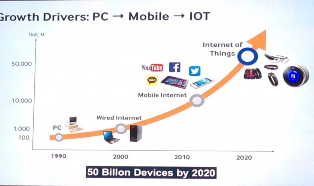
We have already heard a lot about how the Internet of Things (IoT) guarantees ten billion devices by 2018. Did you know that these devices would result in the transmission of 190 exabytes (EB) of information in the same timeframe?

Jim Elliot, vice president of memory marketing at Samsung SSD, puts the magnitude in perspective: “Five EB is the memory needed to store every bit of data generated from the dawn of humanity to 2003.”
By the time of the next FIFA world cup, this number would have gone up almost 20 times to 190 EB. That is a lot of data; where do we store it?
SSD’s glowing track record
More than a decade ago, NAND memory began to revolutionise consumer electronics. It enabled the iPod to disrupt the portable music player device, by driving the Walkman, and naturally the audio cassette too, to obsolescence.
Its effect on hard disk drives has increased over the past few years, with many people now using solid-state drives (SSDs) inside computers, laptops and even as backup solutions. Ultra-portable computer users now use secure digital eXtended capacity (SDXC) cards the size of a 10-rupee coin as their sole backup solution.
“In the data centre and server space, stacks of servers running on hard disk drives (HDDs) have been displaced by NAND flash ubiquity,” adds Jim.
In the last 14 years, the ability to improve a single gigabyte (GB) of memory has improved by over 64 times.
Can SSD technology handle the data explosion?
Conventionally, the industry created new solid-state memory products with a higher capacity than previous generations by cramping more and more cells into the same conventional planar NAND architecture. In this way, we have moved from solutions that could store only a few megabytes to current products that can store hundreds of gigabytes.
However, the shrinking form-factors of devices demands smaller solutions with greater storage. And, the challenge is that the industry cannot continue with the same old methods to meet market demands, as the density limits for packing more into the same planar space have been hit!
As chip manufacturers move to smaller geometries in semiconductor manufacturing processes, new problems and design challenges crop up that hinder the functioning of the chip. Adopting the 10 nanometre (nm) process for memory was difficult with conventional designs, especially due to problems like cell-to-cell interference at such close proximity and challenges with photolithography. Things had gotten so small that even light found it difficult to shine through the smaller patterns in this node.
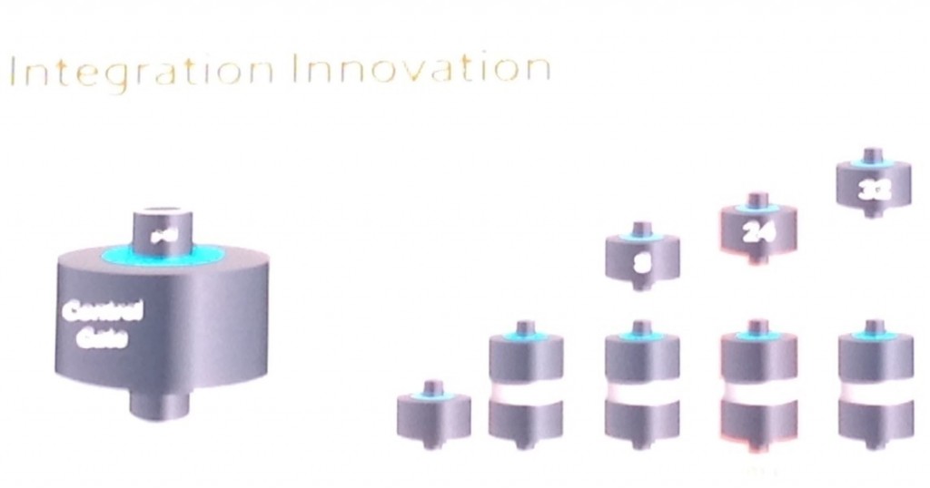
Microprocessor vendors implemented three dimensional integrated circuits (3D-ICs) in their chips, but this concept was not directly implementable in memory technology, since the elements differed between transistors and cells. All until Samsung R&D engineers led by Kye Hyun Kyung, senior vice president for the flash design team, figured out the solution.
Thinking in 3D
The new 3D Vertical NAND (V-NAND) technology for memory makes use of a vertical design to stack memory cells on top of each other. Therefore, rather than reducing the length and width of cells, the designers were able to stack layers of memory cells on top of each other in a 32-layer cylindrical cell structure, while maintaining architectural elements that relate to performance in terms of reliability and speed.
This technology enables devices to outperform the previous generation of memory devices, which were based on the 20 nm planar NAND flash technology.
The new technology was successfully implemented in the latest line of SSDs, which are already in production. It has made it possible to place 43 billion cells in a 128 GB three-bit NAND flash memory device, successfully allowing the product to bypass the restrictions of the smaller 10 nm process.
As an example, this technology has enabled Samsung to come out with an SSD family that holds up to a terabyte (TB) of data while outperforming the competing devices in the market. The fact that the vendor gives a 10-year warranty with this device gives an idea of how SSD reliability has also gone up.
Overpowering the challenges
As we move to 10 nm processes for memory technology, memory cells begin to be placed really close together on the chip, giving rise to varied difficulties, as explained earlier. The material, structural and integration innovations implemented to develop 3D V-NAND overcome these to a large extent.
Cell-to-cell interference. Cell-to-cell interference in memory is a state wherein a cell is affected by the activity of neighbouring cells. When a group of cells in the same area are active at the same time, their behaviour begins to affect each other resulting in performance deterioration. This is due to the electrical charge from one cell coupling on to the closest cell, which results in a change in data on the second cell.
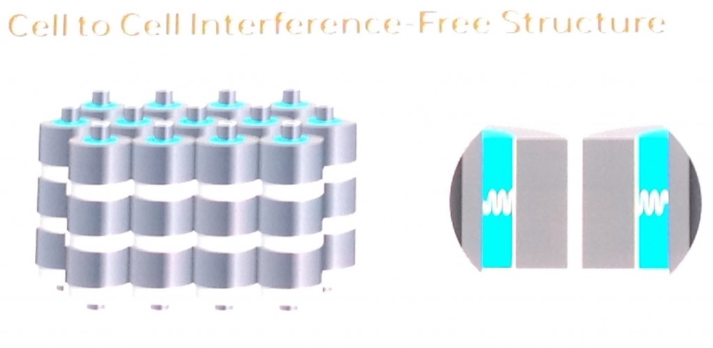
We can draw an analogy with apartment complexes where you can often hear your neighbour talking or working in her house! This unintentional and unavoidable eavesdropping is what is called cell-to-cell interference in tech parlance.
As the space between cells becomes smaller, the chance of data corruption between these cells dramatically increases to the point that cell-to-cell interference becomes a significant problem.
