8. Explanation of how the internal clock frequencies are derived—using phase-locked loop (PLL) or delay-locked loop (DLL) with the input clock. Also, explain how the global clock buffers are used. Mention clock signals with their frequency and voltage levels that are driven out of the FPGA for external peripherals
9. A simulation environment setup for the design (called ‘device under test’) with a top-level testbench. A block diagram indicating how the clock source, reset and pattern generators, and bus functional modes are connected to the top-level module under testing will be helpful here. Mention how log filesare used to register the activity of the required signal
10. Make a page with the heading ‘FPGA Synthesis and Resource Utilisation.’ Keep it blank with a note that once the final implementation is done, this page will be updated
11. Under the heading ‘Timing Analysis,’ mention the major timing parameters of the control signals to be maintained, with a timing budget and waveform drawn manually or using timing analyser tool. Mention the major timing constraints that will be used in the UCF or QSF filesof the design
As mentioned in Step 1, the FPGA team members, hardware and software team members and architects should review the document at several stages before releasing it to the client.
Step 3: Design entry and functional simulation
Each module owner should develop a testbench for his module, capture simulated waveforms or assertion-based log report, and get it reviewed by the team lead. Before going for synthesis, every module should be verifiedthoroughly for functionality using simulation. Regular code review will help to reduce errors and simulation time. Once the simulation of individual modules is done, the next step is to integrate the module and do full-system-level functional simulation with assertion-based log report.

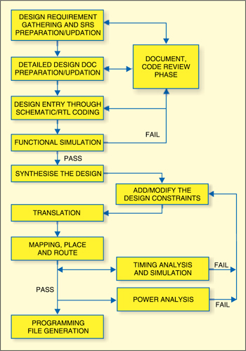
Fig. 2: FPGA design flowchart
Step 4: Synthesis
If the functional simulation satisfie the requirement, the next phase is synthesis.
In this phase, the integrated project is synthesised using a vendor-specificsynthesis tool based on the optimisation settings. Whenever RTL is modifed, it is always good to complete Step 3 with unit-level and full-system functional simulation. Always follow vendor-specificcoding guidelines and library modules for better optimisation of the design.
During this phase, synthesis tools verify the design for syntax errors and do block-level floor planning.
Step 5: Adding design constraints
Once synthesis is complete, constraints can be added to the design. These constraints are usually included in a separate fle where the designer lists out the signal with its corresponding FPGA pin number, I/O voltage levels, current-driving strength for output signals, input clock frequency, hard block or module location, timing paths to be ignored, false paths, other IP-specificconstraints recommended by the vendor, etc. This information is passed on to the placement phase.
Step 6: Placement and routing phase
Before routing, the synthesis tool maps the buffers, memory and clock buffers to the specificvendor libraries. That is, in this phase, logical blocks are translated into physical fileformat. Then, in the place-and-route process, the tool places and routes the design considering the user constraints and optimisation techniques. Timing simulation can be done at this stage to verify the functionality, so that the design meets all the functional and timing requirements.
Step 7: Programming file generation
After obtaining a satisfactory timing and functional behaviour of the design, it is time to generate the bit filethat is downloaded to the FPGA to test the functionality on the board with actual peripherals.
For each stage, the tool will provide the corresponding report files,using which the designer can analyse time delays, power, resource usage, unrouted signals and I/O pins list.
In short
To summarise the above points, the FPGA design flowis shown as a simple flow-chartin Fig. 2. There may be minor variations in the design fow during the requirement stage and the design and document preparation phase, from one organisation or project to another, but the overall FPGA design flow remains the same.
The author is a senior tech lead in Dexcel Electronics Designs, Bengaluru. He has hands-on experience in Xilinx, Altera and Actel FPGAs


