This article discusses the electrical power(s) routed on the PCB and its Integrity down the road as it propagates from VRM to Device, aka Source to Load.
Key Takeaways
- Basics of PI
- Cause of PI Issues
- Impact of Poor PI
- Mitigation
Introduction
With the growing demand for faster and more efficient Hardware, particularly in the dynamic environments of consumer electronics, AI/ML, data centers, edge computing, and telecom/networking systems, power delivery poses a complex and significant challenge for designers.
Devices running at over GHz frequencies require faster and higher load transients, which underscores the essence of stable power for the uninterrupted operation of hardware systems.
Power integrity is no longer a concern only at the PCB level but also at the System/Module level. Poor power integrity could lead to Signal Integrity problems such as power supply-induced jitter and, eventually, EMI compliance failure.
This underscores the need for a holistic approach to Power Integrity, where the PCB and the package must work harmoniously to ensure stable power delivery to interconnects.
This is articulated to provide a fundamental conceptual understanding of Power Integrity for Electrical and Electronics Engineers.
Although Board Designers often have limited control over packaging, they can still take steps to ensure their PCB and component packages function together effectively.
The guide will cover essential strategies for maintaining power integrity, including stack-up design and capacitor selection.
Fundamentals of Power Integrity
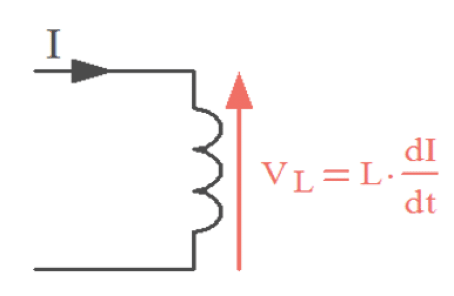
Switching Noise is induced when the state of current changes or transits from low to high or vice versa. As we know, a change in current passing through an inductor causes a voltage.
This means that the change in current in one signal-return path loop can produce noise voltage in an adjacent signal-return path loop, which we define as crosstalk in the electrical world.
This noise worsens when the return paths are shared between the two current carrying loops and better when the signal-return path loops are closely connected and far apart.
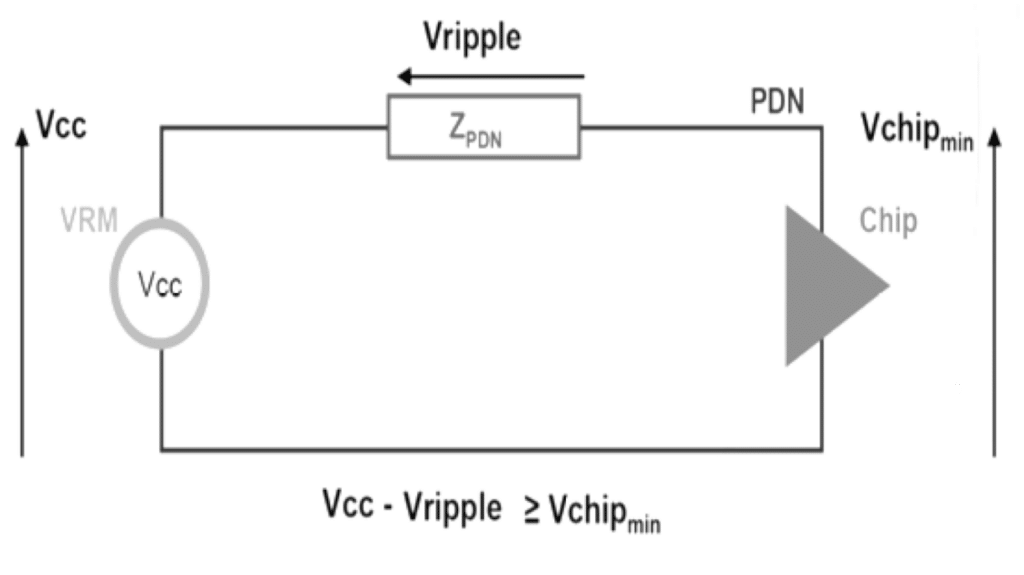
The power-path (+) routing potentially adds another switching noise to the mix. This switching noise is induced by the loop inductance of the power distribution path, starting from the voltage source to each pin/pad of the IC, termed the power delivery network (PDN).
This switching noise is more significant in breadboard-based circuit interconnects than in Printed Circuit Boards.
Switching noise induced along the delivery network is dominated by the loop inductance of the power-ground path.
The device could be impacted by Self-aggression or Mutual aggression, meaning earlier if the device is victimized due to its load and later if the load of other device(s) connected to the power rail causes it.
Where Does Power Rail Switching Noise Come From?
A switching current through an ideal inductor creates a voltage noise across it (illustrated in Figure 1). The Power Delivery Network, as described earlier, the path between Source and load, typically acts as an inductor from MHz (depending on SFR) and onwards.

The active devices, such as microcontrollers, microprocessors, cameras, modems, etc., perform their functionality by sinking current. This current sink is time-varying, meaning it keeps changing from the power rail over a period based on need.
This varying current causes Switching Noise due to the PDN’s inductance. A voltage drop across PDN will momentarily cause the voltage at the device IC pin to drop below the VRM voltage during the dI/dt, in other words, current transients, termed as Rail Collapse.

Impact of Poor Power Integrity
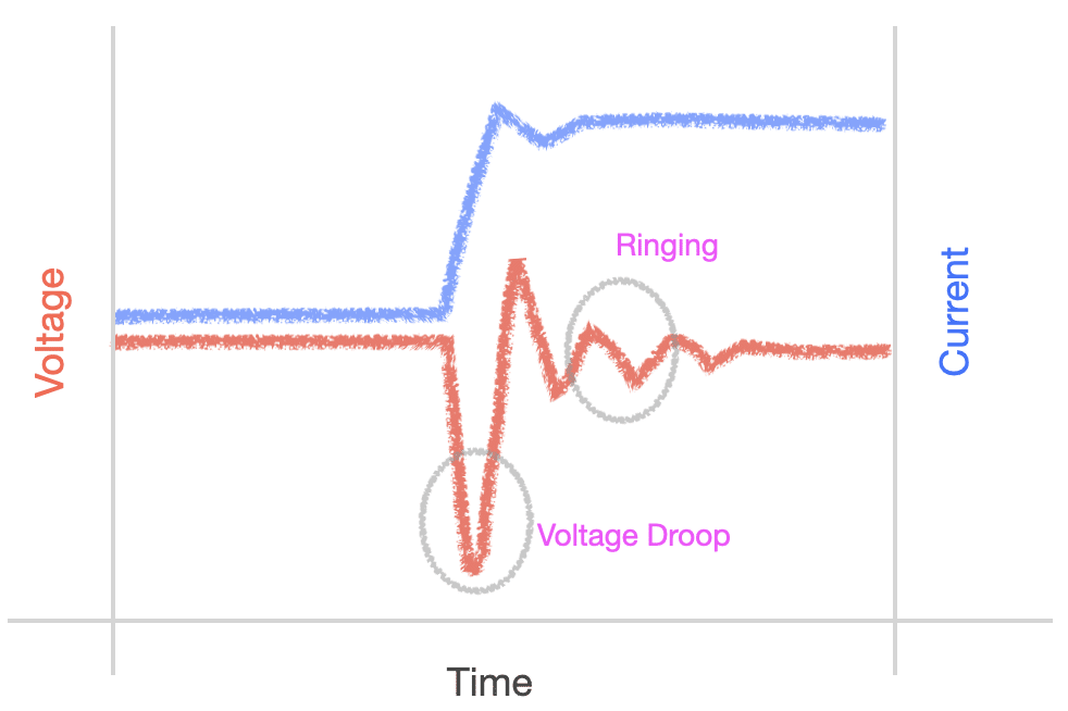
The voltage drop across PDN in an AC condition is called Vdroop. When this droop exceeds the acceptable limit, the device will malfunction.
Figure 3 shows how voltage dips during current transients and takes a certain time to settle down. Given that PDN can be illustrated as a combination of capacitance and inductance, the load current profile might excite some LC resonances, which causes ringing on the IC’s power rail pins.
As shown, ringing occurs during settling time, a combination of overshoot and undershoot. Ringing is a high risk for EMI-EMC and sensitive applications where analog-to-digital conversion occurs.

Board-level circuit designers rarely have the luxury of reducing the transient current from the load IC, as it is required to perform the intended transistor-level circuit function. This implies that the most viable way of reducing power rail switching noise is to drastically improve the loop inductance from source (VRM) to load (IC).
Best Design Practices
This article focuses on a handful of guidelines. Here are some fundamental principles to remember:
- Add a few ‘uF’ of bulk capacitors on the input side of the VRM to shunt the noise coming in, which could also show up at the VRM’s output (if the VRM PSRR circuit is insufficient)
- Place a few ‘uF’ of decoupling/bypass capacitors rated for 2x the rail voltage and be physically close to the package leads as possible.
- For the Power path, route a shorter, direct, wider trace (or copper puddle) between the IC leads and the decoupling capacitor to reduce the loop self-inductance between them.
- Use a continuous ground plane/return path (-) on the adjacent power (+) routing layer.
- For decoupling, choose surface-mount (SMT) MLCC capacitors, never the ones with leads, as they have 10x the loop inductance.
- To mitigate/oppose the change in current, put a series ferrite inductor rated for 2x the rail current at the output of VRM.
Summary
Power integrity resides in the white space of circuit schematics, where engineers might not happen to pay much attention to it.
In Hardware systems, as ICs and devices demand higher load transients and switching rates, more than just making the right net connections and selecting the right components, designers should pay greater attention to component placement and routing/layout, which impacts Power Integrity the most.
Poorly selected PCB stack-up and routed layouts increase the cost of fixing and the time to market as they might need a complete re-spin of the board design, as Silicon re-design is not ideal.
Ensuring end-to-end/Full-Channel Power Integrity across PVT corners has become crucial for reliable system performance.


