Your smartphone detects defects smaller than a virus using AOI, laser, and X-ray systems. These machines don’t just see—they think. These innovations, from AI-driven defect detection to Nano-CT systems revealing hidden flaws, reshape quality control in electronics manufacturing.
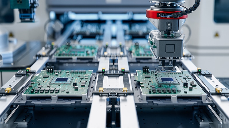
Table of Contents
Ensuring the quality and reliability of printed circuit board assemblies (PCBAs) is vital in electronics manufacturing. Automated optical inspection (AOI) systems are central to this effort, detecting defects throughout the assembly process. With the increasing complexity of PCB designs, AOI technologies have evolved, integrating optical, X-ray, and laser systems to improve detection. This article examines the strengths and applications of these three leading AOI technologies in PCBA production.
Optical AOI: The foundation of visual inspection
Optical AOI systems use high-resolution cameras and advanced algorithms to inspect PCBAs for surface-level defects, such as:
Component misplacement
Ensuring components are correctly aligned and positioned
Solder joint issues
Detecting insufficient, excessive, or bridged solder

Missing components
Identifying areas where components are absent
Polarity errors
Verifying the correct orientation for polarised components
These systems rely on visible light, typically supplemented by LED lighting, to enhance contrast and highlight specific features. Modern optical AOI machines employ advanced imaging techniques, such as 3D imaging, to capture depth information and improve accuracy in detecting subtle defects.
However, optical AOI has its limitations. It excels at inspecting surface mount technology (SMT) components. Still, it faces challenges with solder joints hidden under packages like ball grid arrays (BGAs) or components on densely packed boards where line-of-sight is obstructed.
X-ray AOI: Peering beneath the surface
X-ray AOI systems address the limitations of optical inspection by enabling non-destructive analysis of solder joints and internal structures. They excel in identifying:
Hidden solder defects
Voids, cracks, or insufficient solder in BGAs and other hidden joints
Internal component damage
Issues within components that might not be externally visible
Multi-layer PCBs
Manufacturing flaws within stacked layers of a PCB
Using either 2D or 3D imaging techniques, X-ray systems provide unparalleled visibility into the subsurface structures of PCBAs. Although slower and more expensive than optical AOI, they are indispensable for fault-critical sectors like aerospace and medical devices, where fault tolerance is minimal.
| New AOI Trends and Their Benefits | ||
| Trend | Detail | Innovation |
| AI and machine learning integration | Leveraging AI/ML for defect classification and adaptive learning to reduce false positives | Systems can learn from operator feedback, improving accuracy over time |
| 3D imaging and inspection | Use 3D imaging to detect solder joint defects and height measurements accurately | 3D AOI can inspect components from multiple angles, providing a holistic view. Examples are Koh Young Zenith UHS, CyberOptics SQ3000 and SAKI 3Di Series |
| High-resolution cameras | Cameras with resolutions up to 25 MP or higher can be deployed for precise inspection | Enhanced image quality and detailed defect detection. Examples Mirtec MV-7 Omni and PARMI SIGMA X Series |
| Deep learning algorithms | Advanced algorithms for feature recognition and anomaly detection | Ability to detect subtle or non-standard defects. Example: Omron VT-S10,ViTrox V310i |
| Edge computing | On-device data processing for real-time inspection | Reduces latency and improves system efficiency |
| Connectivity and IIoT (industrial internet of things) | Integration with factory networks for real-time monitoring and analytics | Enables predictive maintenance and smart manufacturing |
| Large-format PCB support | AOI systems are capable of inspecting oversized PCBs | Accommodates advanced designs and larger assemblies. Example: Test Research, Inc. TR7500QE |
| Dual-lighting technology | Use multiple lighting sources to enhance defect visibility | Improves contrast and identification of subtle defects |
| Software-defined AOI | Flexible software updates to adapt to evolving manufacturing needs | Extends system lifespan and adapts to new component designs |
| High-speed inspection | Systems optimised for fast throughput without compromising accuracy | Critical for high-volume manufacturing environments. Nordson YESTECH FX-942 |
Laser AOI: Precision meets depth measurement
Laser-based AOI systems represent a newer addition to the inspection toolbox, offering capabilities that complement optical and X-ray systems. By using laser triangulation or interferometry, these systems: