


Historically, ICs have followed Moore’s Law, doubling logic capacity every two years while costing half as much with each new generation of process technology. Today, Moore’s Law is suffering from mounting die costs, while no longer delivering traditional performance increases or keeping pace with the growing demand for increased bandwidth and capacity.
The latest technologies and approaches have set out to achieve ‘more than Moore’ to enable next-generation silicon scaling at the current-generation process technology. The process of making chips smaller and smaller is becoming increasingly complex, utilising the most advanced capabilities of physics, chemistry, electrical and mechanical engineering among other disciplines.

Every aspect of chip manufacturing latest in Chip fabrication technology is continually improved to manufacture smaller devices with better performance. Most semiconductor manufacturers and their equipment and materials suppliers spend a significant portion of their revenues on research and development.
New technology advancements
A ‘triple threat’ of new complex technology advancements faces the industry—three-dimensional interconnect (3D IC), extreme-ultraviolet lithography (EUV) and 450mm wafers. Despite highly-evolved industry collaboration processes such as the International Technology Roadmap for Semiconductors (ITRS), SEMI International Standards and the growth of international research consortiums, major process milestones in lithography, wafer sizes and new transistor architectures remain unclear and have made coordinated industry planning more necessary than ever before.
The most important challenges in semiconductor manufacturing are the move to larger (450mm) wafers, the commercialisation of EUV, and various ways to utilise three-dimensional (3D) device structures and packaging technologies.
Move to 450mm wafers
Periodically, the industry adopts a larger wafer size standard to improve the efficiency and affordability of manufacturing. These manufacturers claim that larger wafers are necessary to keep pace with Moore’s Law’s cost targets.
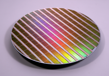
The industry-wide cost of R&D to transition to a larger wafer size (including the development of new manufacturing tools) is estimated between $16 billion and $30 billion. Some chipmakers have already committed to advancing this transition.
Intel has announced that its D1X fab in Oregon will be 450mm-compatible. The fab is expected to complete in 2013. Taiwan Semiconductor Manufacturing Company (TSMC) plans to build a 450mm pilot line by 2013-14. Interuniversity Microelectronics Centre, Belgium (IMEC) and International SEMATECH Manufacturing Initiative (ISMI) have well-established programmes focused on the challenges posed by manufacturing with 450mm wafers, and Albany, NY based Colleges of Nanoscale Science and Engineering at SUNY Polytechnic Institute is expanding facilities to encompass 450mm R&D programme.
EUV lithography rollout
EUV is a widely debated transition. Moving from deep-ultraviolet lithography to extreme ultraviolet lithography is a major shift. Industry players continue to make tremendous investments to develop the next-generation technology that will scale devices to smaller dimensions. The EUV lithography rollout is complex because it is intertwined with the 450mm planning challenge—reinforcing the need for more transparency in planning and funding.
Emerging architectures and technologies
Traditional planar CMOS transistors start to run into severe electrical current leakage issues past sub-20nm nodes. To overcome these issues, manufacturers of both logic and memory devices are looking at a variety of alternatives.
For logic devices, two alternatives have come to the forefront: Fin-type field-effect transistors or FinFETs, and ultra-thin-body silicon-on-insulator or UTB-SOIs (also referred to as fully depleted or FD-SOIs). Intel has already announced its first FinFET device. Other device manufacturers continue to look at both the alternatives.
Memory device manufacturers are looking at alternatives to today’s charge-based memories including resistive RAMs, spin-torque transfer RAMs and phase-change memories.
These new memories will increase the speed of memory devices while at the same time lowering the overall power requirements.
3D and 2.5D packaging
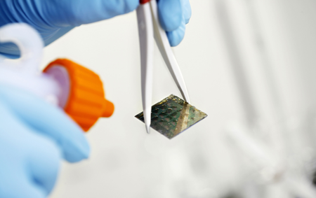
3D interconnects using through-silicon vias are critical for meeting the challenging performance and power target demands of wireless, networking, computing and graphics devices, not to mention the consumer demands for small portable devices.
3D packaging saves space by stacking chips and using through-silicon vias to connect the chips as opposed to traditional wire-bonding methods. The chips can be of the same type as in hybrid memory cubes, or an integrated stack of heterogeneous devices.
2011 was a breakthrough year for 3D ICs, as companies like IBM, Micron, Samsung, ST-Ericsson and Xilinx grabbed headlines for deliver-ing the industry’s first 3D ICs based on through-silicon via technology or disclosing their 3D IC R&D plans.
Specifically, the benefits of 3D IC innovation are:
1. Connectivity. 3D enables thousands of low-latency, low-power die-to-die connections that provide 100x bandwidth/watt of conventional printed circuit boards (PCBs) or multi-chip modules.
