So, where does the paradox lie? Why a technology that is so promising at the concept level has failed to scale up when it comes to its mainstream application in the electronics domain? Enumerating a few reasons, Kolstov says, “The research in molecular nano-electronics is unfortunately very sensational. What I mean is that a research group may measure some effect from one device and write a very popular paper. However, this result has limited use for industrial community since it may not be reproducible, and in some cases is simply wrong. Some recent publications (http://www.nanotechia.org/global-news/is-there-plenty-of-room-at-the-bottom-for-nanomanufacture) argued that some applications of nanoelectronics may never be manufacturable.”
“If we look at the developments so far, it won’t be wrong to say that nanoscience is both futuristic and here today,” affirms Dr Canton. While it is true that the progress made so far in this domain has still not been too fruitful, yet there are areas where the application of nano-science has led to interesting results. Dr Canton enumerates, “Molecular electronics have been shown in the Quantum Computing Lab of Stan Williams at HP to be possible. IBM has done extensive work in nano computer chip development that will likely extend silicon’s life as a chip platform. Mercedes uses nano on coatings for autos to protect the driver. Having said this, nano is emerging and the potential is great, but it is in the early stages.”
Looking beyond processors…
The relevance of nanotechnology and nano materials for reducing the size of transistors can’t be ignored. “Carbon technologies using carbon nanotubes (CNTs), graphene or other allotropes are becoming more and more relevant in this race to continue the Moore’s law,” opines Dr Denis Koltsov. But it would also be worthwhile to explore a few other areas in the electronics space where nanotechnology can potentially have its influence. Let’s take a look at a few of such domains.
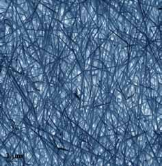
Digital displays. The quality of digital display screens in electronic devices can be improved by reducing the power consumption while decreasing the weight and thickness of the screens. Nano research projects are underway to make use of electrodes made from nanowires to enable flat panel displays, which are likely to be a lot more thinner than the current flat panel displays. “CNTs, which are up to 100-times stronger than steel, and yet only one sixth of its weight, are also being used to direct electrons to illuminate pixels and to develop light-weight, millimeter thick ‘nanoemmissive’ display panel,” informs Rossum. A company called Rosseter in Cyprus is already producing them for commercial use because of their rugged chemical, physical and mechanical properties.
MIT researchers have also created a quantum dot-organic light emitting diode (QD-OLED). While the traditional LCDs are lit from behind, the quantum dots have the capability of generating their own light, and these dots can be manipulated to emit any colour imaginable, with no range limit as seen with traditional devices.
For larger memory sizes. With consumers demanding electronic devices such as music players, mobile phones and computers with gigabytes of memory, the future electronics devices will surely need even larger memory sizes. “The current storage technologies, like Flash memory technology, has an upper-size limit as well as a rewrite limit (between 10,000 and 100,000 writes). Thereafter it will no longer be able to store data. To gear-up to meet with this requirement, multiple examples of memory technologies are being explored that use more exotic materials than what is used in production today,” says Mayberry.
Nanosized magnetic rings are being tried to make magnetoresistive random access memory (MRAM), which research has indicated may allow memory density of 62 GB per square centimetre (400 GB per square inch). Research is also on for using microelectro-mechanical system (MEMS) techniques to control an array of probes, whose tips have a radius of a few nanometres. These probes are used to write and read data onto a polymer film, with the aim of producing memory chips that have a formidable density. There is also ongoing research for the use of nanosized ‘dots’ of nickel, which it is hoped could be used to store terabytes of data, even for home and personal users.
Rossum says, “There are many ideas of using nano features in non volatile memories—molecular structures, metallic nanodots, organic molecules, nanostructured materials and so on. Although their applications are not yet mature, it is still an interesting avenue of research.”

In making existing technologies better. “The developments in nano-technology as a sector have already shown us that this new technology is not only about doing things better, faster at a smaller scale, but also about adding new functionality to existing technologies,” says Kolstov.


