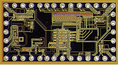
“Optics may allow interconnects to continue to scale to match the processing ability of future electronics chips, though very low-energy optoelectronic devices and novel compact optics will be needed.”
—David A.B. Miller, Fellow IEEE
The performance of silicon CMOS chips is improving because of reduction in the feature size of integrated circuits. We discuss here the current performance and future prospects of interconnection to high-speed VLSI silicon CMOS chips.
What is interconnect?
Electrical interconnection is a medium through which electrical signal propagates from source point to the destination point. In the current scenario, most chips are made by using interconnect wire. By using interconnect wire we can integrate many circuits or devices so that the signal can propagate from one device to the other devices.
Interconnect is made by using circuits like MOSFET and BJT, or electrical parameters like resistance (R), capacitance (C), inductance (L) and conductance (G). Using electrical interconnect leads to some problems as the wires are connected through the devices. The major problems are low capacity and density, very high power dissipation, induced crosstalk noise, delay and bandwidth problem, and timing uncertainty. This is because of the coupling capacitance generated between coupling nodes of two interconnect networks.

The basic general structure of on-chip interconnects is shown in Fig. 2(a). It shows electrical components such as R, L and C in a block connected to another block, making the interconnection system. In a single CMOS silicon chip there are many interconnect wires but these are placed a minimum distance apart.
In Fig. 2(b), the effect of coupling capacitor between the two networks is shown. Minimum feature size of the devices increases coupling between the coupling nodes of the two interconnect lines. Consider the situation in Fig. 2(b) where the input of an inverter is close to an interconnecting line. A parasitic coupling capacitance (CC) exists between the two, so applying a voltage pulse to one line will cause a change in the voltage in the other.
There are three types of interconnects: local, semi-global and global. Local interconnects have a delay of less than one clock cycle, while global interconnects typically take longer than one or two clock cycles. Local and global interconnects are used for short-distance communication. But for long-distance communication, electrical interconnects (local and global) fail to give a good result. So the performance is increased by using a newer technology called ‘optical interconnect.’
Interconnects may be classified as ‘off-chip’ interconnect and ‘on-chip’ interconnect. Off-chip interconnects deal with interconnection of wires between two and more external devices and circuits. On the other hand, on-chip interconnects deal with interconnection of wires into the internal circuitry of one particular chip. Here, in this article, we will discuss only on-chip interconnection.
In the current scenario the performance of electrical interconnects has been improved by changing the technology used to fabricate the wiring layers on silicon CMOS chips.
What is optical interconnect?
Optical interconnect is a medium through which the signal flows in the form of optical rays (light), the medium being an optical fibre, waveguide, etc. Optical wires are capable of much higher bandwidth of 10 Gbps to 100 Gbps. If we talk about the scaling process in VLSI system—reduction in the feature size of transistors—performance of the wire used for electrical interconnect has not improved significantly because of induced noise, delay and high power dissipation. So to improve the performance of the system, we will have to make the silicon CMOS circuit’s performance much better than the electrical interconnect’s. Optical interconnect has the solution to these limitations and can be used for communication between future CMOS circuits.
As shown in Fig. 3, first the electrical signal is converted into an optical signal by using an optical modulator imposed by laser or any optoelectronics device like LED or photodiode. The signal propagates through the optical cable using waveguide. At the receiver side, the photodetector receives the optical signal and converts it into an electrical signal and amplifies.
By using optics many physical problems related to interconnects can be solved. Optics may solve design problems such as crosstalk noise, bandwidth, isolation and impedance matching, and also reduce problems associated with long-distance communication.
Need for optical system
Two important parts of an on-chip optical interconnect are optical devices called ‘optoelectronics devices’ and optical system called ‘medium.’ Here we discuss some basic requirements of an optical system for on-chip optical interconnects. There are two broad categories of the optical system: ‘guided-wave’ optical system and ‘free space’ optical system.


