


For guided-wave optical system, one can use a thin optical fibre cable, waveguide etc. An optical fibre having a diameter of up to 10 µm can be used for on-chip optical interconnect. It has many advantages over other devices such as:
1. No crosstalk inside the optical fibre cable
2. Higher bandwidth, therefore it can operate at a higher data rate
3. Reduced loss due to signal attenuation
4. Small size and light-weight
In waveguide approach, one has to use a waveguide having a diameter of up to 10 µm for on-chip optical interconnect system. Smaller optical guides of the order of micrometre size should have low enough loss so that the propagation loss does not become a big issue for the chip. So for simplicity we connect the waveguide from the central area to the chip to the edges. Whether such guides could handle the internal on-chip interconnects strongly depends on the architecture.

The other approach is to use a ‘free space’ system where multiple light beams can go in and out of the chips, usually in the form of arrays. So arrays of beams go into and out of the chip. Free-space approach can easily handle a large number of arrays of beams. So for high resolution and focusing on the scale of micrometre size, we use an ordinary lens. Optical elements are fabricated using lithographic patterning. These can generate very large regular arrays of spots from a single laser beam and implement a variety of quite complex regular interconnection patterns.
Requirement for optoelectronic devices
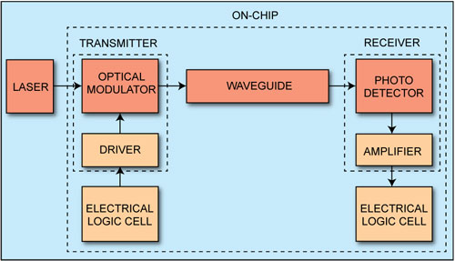
As shown in Fig. 3, an on-chip optical interconnect system consists of transmitter driver circuit, optical channel and receiver circuit. Here p-i-n photodiodes and metal-semiconductor metal (MSM) photodetectors work as the receiver circuit and vertical-cavity surface-emitting laser (VCSEL) and quantum-well modulator work as the transmitter for optical output. The photodetector in the receiver part converts optical energy into electrical energy. In the next step, this electrical signal is amplified by the amplifier circuit. So MSM photodetector gives a fast response and excellent quantum efficiency.
Optical output devices and transmitter circuits. Quantum-well modulator and VCSEL are important devices for the transmitter of on-chip optical interconnect system. You can also use an LED as the transmitter. It will make the fabrication process easier than with VCSELs and avoid some problems of lasers. We discuss here quantum-well modulator and VCSELs in short.
Quantum-well modulator. These modulators are used in demonstrating actual dense interconnects to and from silicon CMOS chips. They are made in large arrays and require an external beam. This requirement can be considered as an advantage or disadvantage of this system. The external beam is required to generate an array and to separate the incident and reflected beams. So we draw a setup that can easily handle the one-master laser beam. The single-master laser beam can be diffracted into arrays of equal beams by using a diffractive beam generator. Additional master laser beam allows centralised clocking of the entire system. Modulators avoid many of the problems of mode quality, wavelength stability, turn-on delay, power dissipation, etc.
VCSELs. VCSELs have made progress recently, especially with the advent of an oxide confined structure that promises to lower threshold currents. Compared to quantum-well modulators, VCSELs have seen less use yet in systems with large arrays operating with the silicon circuit.
Photodetector and receiver circuit. Detector is a very important part for the receiver’s performance as it converts optical energy into electrical energy. For an on-chip optical interconnect system, the detector should have a low input capacitance if the receiver circuit is to be kept small with not too large power dissipation. Large capacitances mean more sensitive amplifiers have to be used, which introduce a noise that degrades the performance of the receiver circuit while also increasing the power dissipation.
A better approach for optical interconnect receivers is to make the physical capacitance of the photodetector and its connection to the receiver circuit as small as possible. Small capacitance leads to larger voltage swings for a given optical energy, which leads to better noise immunity and improved gain stages. Smaller capacitance also allows use of small, low-power-dissipation transistors in the input stage. To calculate the total capacitance, you need to estimate the gate capacitance of the transistor with which the detector would be integrated. For 90nm CMOS technology node the gate capacitance of an NMOS transistor per unit transistor width is estimated to be 2 fF/µm, and for the 32nm node the corresponding number is 1.2 fF/µm.
To sum up
We have seen various advantages of the optical interconnect system over the electrical interconnect. Optical interconnects solve many of the problems arising in electrical interconnects due to chip-to-chip delay, crosstalk noise, bandwidth, interconnect wire and system synchronisation. Optics may reduce the power dissipation in clock distribution; global on-chip and off-chip interconnects improve the timing. We have found that optical interconnects have a performance that is competitive with or better than electrical interconnects’ and can scale to future interconnect needs.
In conclusion, optics is very promising for dense interconnects to silicon chips. Overall, electrical and optical interconnects, and the many existing and emerging technologies in optoelectronics and optics integrated with silicon CMOS, are likely to play a substantial role in solving major problems in scaling interconnects for CMOS chips in the coming decades.
Kapil Khare is doing M.Tech in Microelectronics and VLSI Design from NIT, Durgapur, West Bengal. Dr Rajib Kar is an assistant professor in the department of Electronics and Communication Engineering at NIT, Durgapur, West Bengal
