Physical design implementation of a very large floor plan with high memory count poses multiple challenges mostly in areas like floor planning, power planning and also turnaround time for tool coupled with memory management. In addition to the huge memory count, variation in the size of memories multiplies the complexity and increases challenges in physical design implementation.
Here we talk about designing with a very high memory count of more than 600 and memories of different sizes with different pin densities, which brings along complexity of floor planning. Due to vivid sizes of memories, power planning is also equally challenging, and care has to be taken that rails are not being removed during this stage. With a large core and huge instance count, the run-times and memory requirements were very high, and this limited what the tool could be used for during flat implementation.
The block contained 21 main clocks and hence building the clock tree and meeting latencies and skew targets was also a challenge. We achieved these targets by using some customisation techniques for CTS.

Apart from this, the blocks had highly skewed floor plans, which don’t lend themselves well to typical optimisation engines, and quite often, congestion and sub-optimal timing and placement complicated the implementations.

Design details
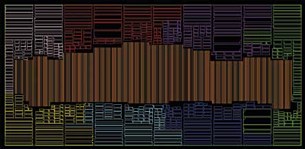
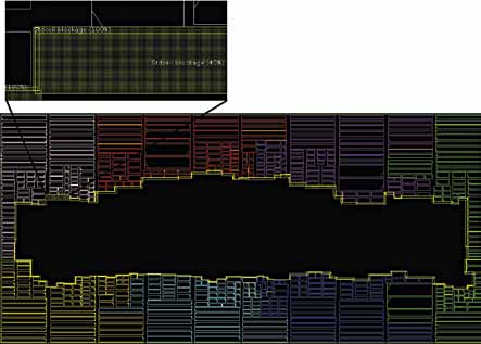
This block is over 12.699 mm2, implemented in 40 nm, with a total instance count of 1.6 million and over 640 macros/memories. The pin count is 652 data and clock pins. The design contains eight metal layers, of which six are used for block-level signal routing and the top two layers are used for power mesh and top-level routing.
The design utilisation is 63 per cent.
The block has 21 main clocks. The maximum frequency is 250 MHz and the minimum frequency is 50 MHz. The design has three modes and seven corners, two for setup and five for hold.
Floor planning challenges
Hierarchy placement. The design is physically flat but the logical hierarchy is maintained. The automatic macro placer identified these top-level hierarchies and the area they needed to be placed. Results of the placer are taken as reference to further the macro placement. Initially, while placing the memories, the individual hierarchy is picked up. Then the internal hierarchies are highlighted and memories with the same hierarchy placed in a stack.
Stack preparation. Stacks of memories are created as the design contains 640 memories. Memories are of vivid aspect ratio and different pin densities, which increased the complexity in stacking. One of the challenges in stacking is that smaller memories have pin counts similar to bigger ones. To tackle this hurdle, smaller memories are kept close to the core area in order to provide them better routing accessibility and reduce congestion.
Channel-width estimation. The main concern while doing this is to identify the approximate channel widths for both the two memories in a stack, and vertical channel width between two stacks of memories. The width of the horizontal channels increases gradually as the channel buffering of any memory stack increases from the block boundary to the block core area.
Pyramidal memory stacking. It’s a special methodology developed to overcome congestion issue. The vertical channel requirement at boundary is lesser than near the core interface because the routing resources and buffering required near the core area is more. This methodology helps tackle this issue by creating a vertical channel in a pyramidal shape from the core to the boundary.
Uniform core area. Another challenge is to create a uniform core area so as to provide better accessibility to memories that are stacked away from the core. The shape of the core area should neither have hillocks nor valleys. In order to achieve this milestone, we tried to control the stack size. The stack size trimming, breaking one bigger stack into two smaller stacks and rearrangement of these stacks helped in achieving a uniform core area.
Timing concerns. The access time of some of the memories is more than half of the clock period. These memories have 30 to 40 per cent contribution to FEP (front end processing) and more than 80 per cent contribution to TNS (total negative slack) if they are placed away from the core area. To avoid this timing criticality, such memories are placed near the core area. This places the related logic near it which, in turn, reduces the wire buffering and slew, and hence the slack. It has a minute impact on congestion, which can be ignored until later stages.