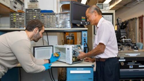
A research professor from Cornell Engineering modified a household microwave oven that assists semiconductor manufacturers to fabricate next-gen semiconductors

Silicon must be doped, or mixed with an extensive amount of phosphorous to meet the need of the desired current and manufacture semiconductors that are efficient and stable. Semiconductor manufacturers have reached a level in which heating to fabricate the highly doped materials using the conventional method does not produce consistently functional semiconductors. The Taiwan Semiconductor Manufacturing Company (TSMC) partnered with Hwang and modified a household microwave oven to selectively control where the standing waves occur. This precision enables for proper activation of the dopants without affecting the silicon crystal. TSMC suggested that microwaves can be utilized to activate excess dopants, but the drawback of using them is that they produced “standing waves” that prevent consistent doping activation. Hence, modification of the microwave oven was necessary.
This invention will transform the geometry of transistors used on microchips. For almost 20 years, transistors have been made to stand up like a dorsal fin so it can accommodate more attributes on each microchip, but with enhanced technology manufacturers recently started an experiment with a new architecture in which transistors are stacked horizontally. The excessively doped materials enabled by microwave annealing would be beneficial for the new architecture.
“A few manufacturers are currently producing semiconductor materials that are 3 nanometers,” Hwang said. “This new microwave approach can potentially enable leading manufacturers such as TSMC and Samsung to scale down to just 2 nanometers.”
Click here for the Published Research Paper


