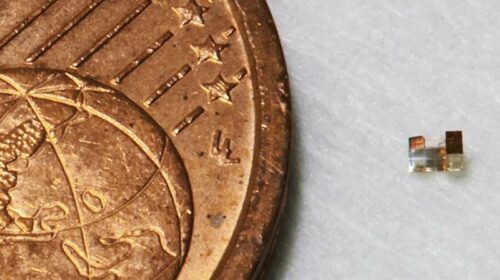
Researchers from Stockholm innovated a newly 3D printing technique that could cost-effectively manufacture customized electronic products with sizes as small as insects

The chip-based microelectromechanical systems (MEMS) are mass-produced in large volumes for hundreds of electronic products but when it comes to manufacturing customized sensors in low volumes such as accelerometers for aircraft and vibration sensors for industrial machinery, in robotics, medical devices, and others, MEMS technologies demand huge investments. Hence, Frank Niklaus, who led the research at KTH Royal Institute of Technology in Stockholm, described that the new 3D printing technique provides a way to overcome the limitations of conventional MEMS manufacturing.
“The costs of manufacturing process development and device design optimizations do not scale down for lower production volumes,” says Frank Niklaus, a researcher at KTH Royal Institute of Technology. The result is engineers are faced with a choice of suboptimal off-the-shelf MEMS devices or economically unviable start-up costs.
The researchers developed a process called two-photon polymerization that can manufacture high-resolution objects as small as a few hundred nanometers in size but not capable of sensing functionality. To form transducing elements, the process used a technique called shadow-masking, which works something like a stencil. They fabricated features with a T-shaped cross-section upon the 3D-printed structure that functions like umbrellas. They then deposit metal from above which resulted in the sides of the T-shaped features not being coated with the metal. This means the metal on the top of the T is electrically isolated from the rest of the structure. The researchers claim that this method takes only a few hours to manufacture a dozen or so custom-designed MEMS accelerometers using relatively inexpensive commercial manufacturing tools. They even assure that the method can be used for prototyping MEMS devices and manufacturing small- and medium-sized batches of tens of thousands to a few thousand MEMS sensors per year in an economically viable way.
“This is something that has not been possible until now because the start-up costs for manufacturing a MEMS product using conventional semiconductor technology are on the order of hundreds of thousands of dollars and the lead times are several months or more,” he says. “The new capabilities offered by 3D-printed MEMS could result in a new paradigm in MEMS and sensor manufacturing. Scalability isn’t just an advantage in MEMS production, it’s a necessity. This method would enable fabrication of many kinds of new, customized devices.”
Click here for the Published Research Paper


