

Sandy Bridge wafer by Intel
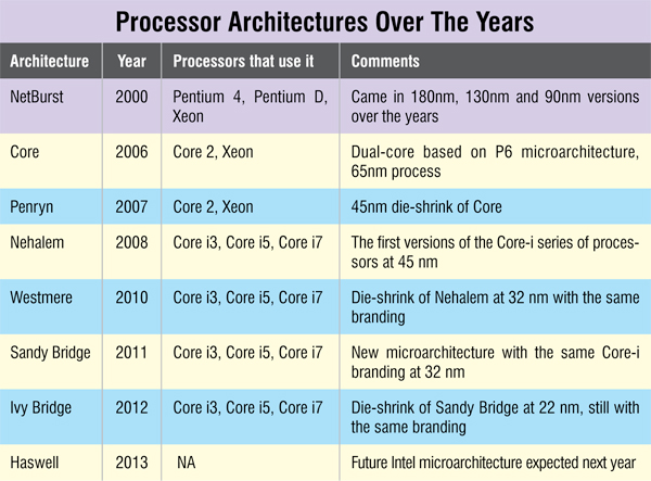
Things tend to get confusing when a chip manufacturer releases a new version just as a device powered by the previous release reaches your hands. Intel’s Core-i branding gets no clearer with each subsequent release of codenamed chips. Since Intel has just launched the die-shrink of the current Sandy Bridge microarchitecture, we realised it is high time we did a rundown of Intel’s CPU microarchitectures and cleared the mist surrounding them.
What are i3, i5 and i7?
These three modifiers form the different line-ups of Intel’s processors.
Core i3. This line-up targets the low-end market. These processors have a lower average thermal design point (TDP) rating which makes them perform cooler, albeit with lower performance. The TDP is the amount of power that the cooling system in a computer should dissipate to ensure proper functioning of the system. The i3 processors are usually restricted to two cores.

Core i5. This is the mainstream variant of Intel’s processors. These processors have a higher average TDP and a larger L3 cache. The cache is an auxiliary memory from which high-speed retrieval of data is possible. This is possible due to its placement on the processor die rather than external to it. Computers have different levels of cache memory: L1, L2 and L3. As the levels increase, the time to retrieve data from them increases along with the amount of data they can store. The i5 processors are available with both two and four cores and are hyper-threading enabled.
Core i7. This is a high-end offering from Intel. Core i7 variants may feature two, four or even six cores along with a larger L3 cache.
Sandy Bridge
Sandy Bridge is the codename for the current serving of microprocessors from Intel. It is based on a 32nm manufacturing process. Intel claims that it offers up to 14 per cent increased performance clock-for-clock over the previous Nehalem microprocessors.
The Sandy Bridge naming scheme continues with the same Core-i branding as before. But one minor difference helps us to differentiate the generations. As you can see from Figs 1 and 2, the generation of a processor can be found out by checking the digit in the thousand’s place that comes after the modifier. So an Intel Core i7-2600K is a second-generation processor, while an Intel Core i7-620M is a first-generation processor (no digit means first generation).
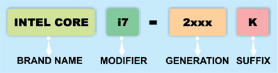
Fig. 1: Intel’s second-generation processor naming
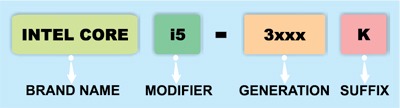
Fig. 2: Intel’s third-generation processor naming
The suffix ‘K’ signifies that the processor can be overclocked for higher performance—useful for gaming enthusiasts and other power users. ‘M’ signifies that it is a processor for use on a mobile platform.
Sandy Bridge is, in fact, a major tock. The architecture underwent a major platform repartitioning with a lot of things being integrated on the die. For instance, the clock generator and the integrated graphics processor now share space with the CPU. All this integration results in extremely low power consumption. The on-die graphics processor called Intel HD Graphics delivers a below par performance, but improved power efficiency through the power-gated GPU. This made Sandy Bridge the best option for portable PCs.
[stextbox id=”info”]What’s Tick-Tock
Tick-Tock is a model developed by Ashwani Gupta of Jones Farm 5 (Hillsboro, Oregon) which has been adopted by Intel Corporation since 2007 to follow every microarchitectural change with a die-shrink of the process technology. Every ‘tick’ is a shrinking of the process technology of the previous microarchitecture and every ‘tock’ is a new microarchitecture.[/stextbox]
Sandy Bridge was released in January 2011.
Ivy Bridge
Intel’s 22nm die-shrink of Sandy Bridge is codenamed Ivy Bridge. Apart from the die-shrink, Intel has utilised a non-planar architecture called tri-gate for the transistor in Ivy Bridge. Marketed as 3D transistors, this technology is claimed to allow the processors to cut power consumption by half and perform 37 per cent faster. Performance wise, the CPU is expected to outperform Sandy Bridge by a whopping 20 per cent.
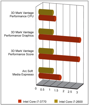
Fig. 3: Performance of Intel Core i7-2600 vs Intel Core i7-3770 (Disclaimer: This representation utilises leaked data to populate the chart)
From Fig. 3, you can see that Intel HD Graphics processor in Ivy Bridge significantly outperforms those in Sandy Bridge processors.
Although Intel factories had to be upgraded to be able to manufacture these tri-gate Ivy Bridge CPUs, the market prices remain roughly the same as a finished wafer costs only about 3 per cent more.
Ivy Bridge also overcomes the shortcomings of the previous line of processors by improving on the graphics processing capabilities. The Intel HD Graphics in Ivy Bridge supports DirectX 11, OpenGL 3.1 and OpenCL 1.1, while also outnumbering the executing units by four to reach a maximum of 16. Intel claims the graphics performance to be 30 per cent better than the previous-generation Intel HD Graphics. Intel HD Graphics in Ivy Bridge comes in two variants: Intel HD 2500 for low-end performance and Intel HD 4000 for better performance.