


New challenges. At 32 nm and below, the intricate process and layout interactions cause failures that are not foreseen by normal simulation tools. Irregularity in logic also causes failures. The very low ‘k’ factors in lithography are also causing problems these days. At the 32, 28 and 22nm levels, this leads to design sensitivies such as hot spots (areas on the die surface that exhibit excessive heating).
Modelling and simulation. Everything including system-level power, gate oxides, etch transfers and line edge roughness has to be measured, modelled and simulated—nowadays even at the atomic level—to spot such problems. Some fabs monitor as many as 50,000 points. Of course, errors do not show up immediately by watching a single wafer. Sometimes, they are found only after monitoring hundreds or thousands of wafers.
From fab to design and back. The key goal behind such modelling and monitoring is to immediately identify problems and their root cause, and correct them at the design stage. All metrology data from the fab has to be fed back to the design centres, and design improvements flown back. This is what most latest diagnostic tools such as those from Mentor Graphics and Synopsys attempt to do. From lithography, manufacturing process to object-oriented process control, everything has to be taken care of at the design stage. This is leading to adoption of many techniques like design-based inspection and design-for-manufacturing (DFM).

“DFM is one area where improvements are being made specifically in phase-shift-mask and OLE process control (OPC) techniques. However, exactly how they help in improving the yield is not clear,” says Prof. Jadcherla.
Identifying problems and improving the yield is no mean task and could take around a year to achieve even for the most experienced companies—as it happened during the introduction of the 40nm process at TSMC, the world’s largest semiconductor manufacturer. When a new manufacturing process is introduced, it is first developed and refined in a test fab and then transferred to production lines in a process called ‘chamber matching.’ This theoretically ensures standard conformity and higher yields. Problems with chamber matching on TSMC’s 40nm lines caused yield problems, thereby making it difficult for the company to match up to the demand for 40nm technology. It took almost a year for them to iron out these problems and plump up the yield of the process to match the previous generation’s.
Improvements in lithography
Lithography is one area in which a lot of improvements have been made, and are expected in the near future—especially due to the advancements made in photonics. As chips become smaller, there is an imminent move from 193 to 13.5nm-wavelength lithography in order to pattern finer features. This is due to a new lithography technology called ‘extreme-ultraviolet’ (EUV) (http://en.wikipedia.org/wiki/Extreme_ultraviolet_lithography) which could allow current chip features to shrink by almost ten times. Since 2009, a variety of EUV tools have been launched, including EUV scanners for process development and EUV light sources.
Apparently, EUV requires a completely new yet cost-effective and reliable light source. Versions have been demonstrated that hit 100W output power, enough for minimal production. However, high-volume manufacturing will require double that figure. A recently launched EUV source from Cymer Inc. of San Diego uses a high-powered infrared laser to bombard a microscopic molten tin droplet as much as 50,000 times per second. The resulting plasma radiates photons over a range of wavelengths. The 13.5nm light is collected and directed into the scanner illuminator. Japanese company Gigaphoton Inc. is also pursuing a similar laser-based approach. The company has announced plans to start shipping EUV light sources this year.
It is expected that by 2012, production systems for volume manufacturing using EUV lithography will be available. However, this is assuming that certain hurdles are mounted. Making masks of sufficiently high quality, for instance, is still a challenge. Another is checking for defects in those masks initially and after use. Companies such as KLA-Tencor Corporation and Carl Zeiss SMT are making mask inspection tools capable of handling 22nm logic node EUV masks. However, these work using 193nm sources, and it is believed that they will work only up to 16nm process technology. So, what after that?
A review of the recently held SPIE Advanced Lithography – EUVL Conference by Vivek Bakshi (http://semimd.com/blog/2011/03/07/2011-spieadvanced-lithography-%E2%80%93-euvl-conference-review/) provides an excellent overview of recent methods in lithography and metrology.
Experiments with newer materials
Silicon has dominated the semiconductor manufacturing space for ages and, frankly, it is still one of the best materi-als for chips. However, new materials are being experimented for newer applications and smaller geometries, but none has moved beyond research to volume production yet. As long as we continue with the same material, improvements will only be incremental.
Electronic devices such as touch-screens, flexible displays, printable electronics, solidstate lighting and thin-film photovoltaics, for example, would be much better off with flexible transparent conductors. Standard indium-tin xide films are unlikely to satisfy future needs due to losses in conductivity on bending and the escalating cost of indium which is in limited supply.
“Recent research related to graphene indicates that it may be suitable as a transparent conductor. Graphene hybrids with carbon nanotubes, for example, may prove to be especially interesting,” explains Prof. Jadcherla.
Some companies have also been experimenting with polymer-based semiconductor manufacturing. Other materials like bismuth telluride and molybdenite have also been checked up. However, carbon nanotubes show much more promise than any other option, although not in the short-term. A lot of disparate but promising research is happening on that front. Last year, IBM revealed carbon nanotube air filters for semiconductor manufacturing. In January, TSMC patented a carbon nanotube bond pad structure and the methods for using it. In February, Prof. Yutaka Ohno from Nagoya University in Japan and Prof. Esko Kauppinen from Aalto University in Finland shared details of a simple and fast process to manufacture high-quality carbon nanotube-based thin-film transistors on a plastic substrate. This can go a long way in producing cheap, powerful electronics. However, it might be years before carbon nanotubes really come into semiconductor manufacturing in a big way.
[stextbox id=”info”]since not much can be done to reduce the actual time of manufacture, the onus has shifted to the design stage. more capable tools and processes are helping to reduce the time taken at this stage[/stextbox]
“Nanotubes and other materials are not yet on the horizon as far as volume manufacturing is concerned. This trend is unlikely to reverse in the next 5-10 years. But yes, a revolution is expected. Carbon nanotubes are expected to become mainstream in a decade,” says Sathe.
Changes galore
There are lot more trends catching up in the space. For example, device makers are moving towards a fab-lite model, whereby they handle only the designing and outsource the manufacturing to foundries, in order to avoid the cost of setting up a fab and the problems caused by changes in technology and demand.
Another trend is the focus on reducing the time-to-market. Since not much can be done to reduce the actual time of manufacture, the onus has shifted to the design stage—more capable tools and processes are helping to reduce the time taken at this stage.
Sathe agrees, “The time taken for manufacturing and post-manufacturing process is generally fixed. Hence the emphasis is on reducing the design cycle time. An approach preferred these days in creating bigger system-on-chips is to reuse or buy intellectual property, and to work with design partners rather than in-house development. The integrated device manufacturers are looking at a faster time-to-market and increasing market share rather than a complete in-house design approach. New methodologies brought in by electronic design automation vendors, e.g., Magma’s methodology to accelerate analogue porting and optimisation, also help in this.”
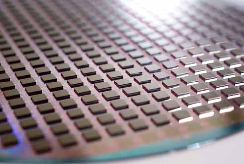
There is also an attempt to move from the current 30.5cm (12-inch) wafers to 45.7cm wafers. The 30.5cm, 300mm wafer-based technology, which itself is kind of new, yields 2.25 times more chips per wafer than the older 20.3cm (8-inch), 200mm wafers, yet they take just about the same time to pass through a factory, reducing the cost per chip and significantly boosting total monthly output. A 45.7cm wafer plant would show a similar reduction in per-chip cost and increase in output. However, as of now, nobody can afford a 45.7cm fab. An industry conglomeration, including TSMC, is looking at how to make 45.7cm fabrication more affordable. The company expects to bring it into operation by 2015. Let us wait and see what other changes happen by then.
The author is a technically-qualified freelance writer, editor and hands-on mom based in Singapore
