A field-programmable gate array (FPGA) is all about programmability of software, hardware, input-output (I/O) and often analogue components too. With better design and programming tools, improved performance and energy efficiency, FPGA usage is proliferating.

architecture uses time as the
third dimension
(Courtesy: Tabula)
Though communications remains the biggest market, FPGAs are also increasingly being used for controlling displays in consumer devices, digital signal processing, software-defined radios, radar systems, situation-aware devices, IoT products and even supercomputing. As a result, companies and universities are pooling their brains and brawns to come up with improved FPGAs, related IP, software and tools. Here is a sample of what is brewing.
Fretting over FinFET. From design companies to fabs, everybody is sweating over the FinFET transistor structure, which is believed to be the biggest development in semiconductor technology in the past four decades! FinFETs are basically 3D structures that rise above the planar substrate. This gives more volume without increasing the planar area. Plus, FinFETs are also estimated to be up to 37 per cent faster, while using less than half the dynamic power, and cut static leakage current by as much as 90 per cent, according to a technology report by Synopsys. They also help overcome performance versus power tradeoffs. Researchers have been working to reduce current leakage through the body when the device is in the state, in order to allow lower threshold voltages.
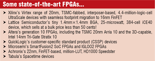
Some research groups have also shown that FinFETs can be scaled by scaling the thickness of the channel. The Korea Advanced Institute of Science and Technology, for example, has demonstrated a 3nm FinFET. It is clear that FinFET is the way ahead for FPGAs too. Xilinx, for example has demonstrated their UltraScale range of all-programmable chips, which takes FPGA technology from 20nm planar monolithic to 16nm FinFET 3D ICs.

Fuelling FPGA innovation. Accelerated processing units (APUs) are often behind the success of FPGA designs. To this effect, AMD’s upcoming Kaveri might be a notable development in the FPGA space. Kaveri pools four CPU cores and eight GPU cores and enables them to work so seamlessly that it has the power of 12 compute cores. This is their first HSA architecture based APU. They claim that adopting HSA, the new processor design standard, will enable engineers to make better use of the APUs for general computing.
Work on on-chip interfaces. It is expected that synthesisable implementations of DDR3, RDRAM, Interlaken and other high-speed interfaces that operate intra-chip and inter-chip will be important for the future of FPGAs. The Interlaken interface developed by Cisco and other original equipment manufacturers (OEMs) is popular as a server and switch interconnect for high-speed Ethernet. However, recently Cavium used Altera’s Interlaken IP core to link Altera FPGAs with its own Octeon processors, demonstrating a new way in which FPGAs with high-speed transceivers can use multi-gigabit interfaces such as Interlaken.
EDA industry leaders are all focussing on developing optimised synthesisable interfaces for systems-on-chips (SoCs). At the recently held MemCon too, it was iterated that, although FPGA vendors would continue to emphasise efficient IP cores for 40- and 100-Gbit Ethernet, Fibre Channel Gen 5 and PCI Express Gen 3, they will definitely be working with EDA specialists such as Cadence, Synopsys and Mentor to offer power-optimised on-chip buses, both for memory interconnect and for links between multi-processor cores.
Embedded networks-on-chips for FPGAs. In February this year, Mohamed Abdelfattah and others at the University of Toronto proposed that, integrating networks-on-chips (NoCs) on FPGAs can improve device scalability and facilitate design by abstracting communication and simplifying timing closure, not only between modules in the FPGA fabric but also with large hard blocks, such as high-speed I/O interfaces. Their design features mixed and hard NoCs, which add less than one per cent to the area of the FPGAs yet run five to six times faster than the soft equivalents.
Their research showed that hard NoCs consume 4.5-10.4mJ of energy per gigabyte of data transferred, which is comparable to the energy efficiency of simple soft point-to-point links in FPGAs, while offering greater benefits. The design is more energy-efficient and space-saving compared to custom buses configured into the fabric by commercial system integration tools.
3PLDs from Tabula. FPGA player Tabula has come up with future-ready spacetime technology, which apparently overcomes the limitations of FPGA’s 2D topologies by using a third dimension to create a class of 3D programmable logic devices (3PLDs). Spacetime uses hardware capable of dynamically reconfiguring at multi-gigahertz rates and the Stylus compiler, which transparently manages this ultra-rapid reconfiguration of logic, memory and interconnect resources throughout the chip. Actually, the third dimension of space is created using time, and hence the name Spacetime!
According to Tabula, “A Spacetime device reconfigures on the fly at multi-gigahertz rates, executing each portion of a design in an automatically defined sequence of steps. Manufactured using a standard CMOS process, Spacetime uses this ultra-rapid reconfiguration to make time a third dimension. This results in a 3D device with multiple layers or folds in which computation and signal transmission can occur. Each fold performs a portion of the desired function and stores the result in place. When some or all of a fold is reconfigured, it uses the locally stored data to perform the next portion of the function.


